HY5DU281622ET
25
26
28
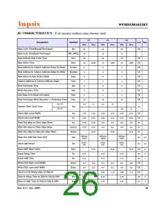
Unit Note
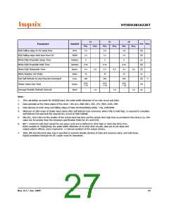
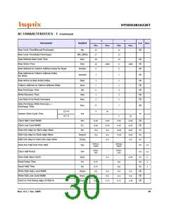
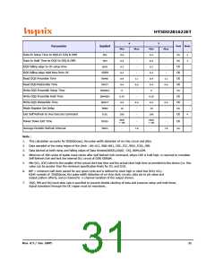
Parameter
Symbol
Min
3.0
3.0
0
Max
Min
3.0
3.0
0
Max
Min
3.0
3.0
0
Max
DQS falling edge to CK setup time
DQS falling edge hold time from CK
Write DQS Preamble Setup Time
Write DQS Preamble Hold Time
Write DQS Postamble Time
tDSS
tDSH
-
-
-
-
-
-
CK
CK
ns
tWPRES
tWPREH
tWPST
tMRD
-
-
-
0.35
0.4
10
-
0.35
0.4
10
-
0.35
0.4
10
-
CK
CK
ns
0.6
-
0.6
-
0.6
-
Mode Register Set Delay
Exit Self Refresh to Any Execute Command
tXSC
200
-
200
-
200
-
CK
4
2tCK
+ tIS
2tCK
+ tIS
2tCK
+ tIS
-
-
-
Power Down Exit Time
tPDEX
tREFI
CK
us
-
7.8
-
7.8
-
7.8
Average Periodic Refresh Interval
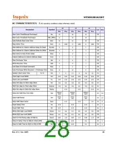
Note :
1. This calculation accounts for tDQSQ(max), the pulse width distortion of on-chip circuit and jitter.
2. Data sampled at the rising edges of the clock : A0~A11, BA0~BA1, CKE, /CS, /RAS, /CAS, /WE.
3. Data latched at both rising and falling edges of Data Strobes(UDQS,LDQS) : DQ, LDM,UDM.
4. Minimum of 200 cycles of stable input clocks after Self Refresh Exit command, where CKE is held high, is required to complete
Self Refresh Exit and lock the internal DLL circuit of DDR SDRAM.
5. Min (tCL, tCH) refers to the smaller of the actual clock low time and the actual clock high time as provided to the device (i.e. this
value can be greater than the minimum specification limits for tCL and tCH).
6. tHP = minimum half clock period for any given cycle and is defined by clock high or clock low (tCH, tCL).
tQHS consists of tDQSQmax, the pulse width distortion of on-chip clock circuits, data pin to pin skew and
output pattern effects, and p-channel to n-channel variation of the output drivers.
7.
DQS, DM and DQ input slew rate is specified to prevent double clocking of data and preserve setup and hold times.
Signal transitions through the DC region must be monotonic.
Rev. 0.5 / Jan. 2005
27

 HYNIX [ HYNIX SEMICONDUCTOR ]