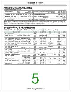
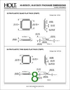
HI-8050/51, HI-8150/51
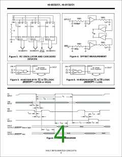
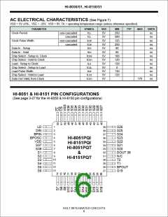
AC ELECTRICAL CHARACTERISTICS (See Figure 7)
VDD = 5V ±5% , VEE = -25V, VSS = 0V, TA = operating temperature range (unless otherwise specified).
PARAMETER
SYMBOL
VDD
MIN
TYP
MAX
UNITS
Clock Period
non-cascaded
cascaded
tCL
tCL
5V
5V
5V
5V
5V
5V
5V
5V
5V
5V
5V
5V
5V
250
500
125
250
80
ns
ns
ns
ns
ns
ns
ns
ns
ns
ns
ns
ns
ns
Clock Pulse Width
non-cascaded
cascaded
tCW
tCW
tDS
Data In - Setup
Data In - Hold
tDH
80
Chip Select - Setup to Clock
Chip Select - Hold to Clock
Load - Setup to Clock
Chip Select - Setup to Load
Load Pulse Width
tCSS
tCSH
tLS
100
120
120
0
tCSL
tLW
tLCS
tCDO
130
120
Chip Select - Hold to Load
Data Out Valid, from Clock
170
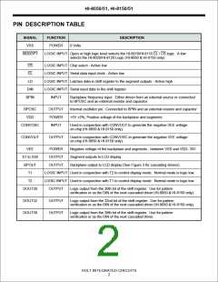
HI-8051 & HI-8151 PIN CONFIGURATIONS
(See page 3-27 for the HI-8050 & HI-8150 pin configurations)
1
LD
DIN
BPIN
BPOSC
39
38
37
36
35
34
33
32
31
30
29
28
27
S26
2
S25
S24
S23
S22
S21
S20
DOUT 38
N/C
T2
3
4
HI-8051PQI
HI-8151PQI
HI-8051PQT
5
VDD
S37
S38
S1
6
7
8
&
9
S2
S3
S4
S5
HI-8151PQT
10
11
T1
BPOUT
S19
12
13
S6
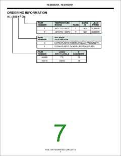
HOLT INTEGRATED CIRCUITS
6

 HOLTIC [ HOLT INTEGRATED CIRCUITS ]