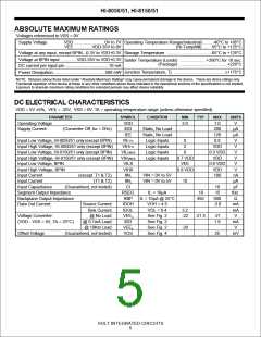
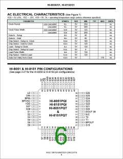
HI-8050/51, HI-8150/51
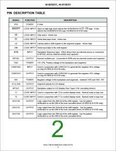
PIN DESCRIPTION TABLE
SIGNAL
VSS
FUNCTION
DESCRIPTION
POWER
0 Volts
8020OPT
LOGIC INPUT Open or high logic level selects the HI-8010/HI-8110 CL / CS logic. A low
selects the HI-8020/HI-8120 Logic (HI-8050 & HI-8150 only)
CS
CL
LOGIC INPUT Chip select - Active low
LOGIC INPUT Serial data input clock - Active low
LD
LOGIC INPUT Latches data in shift register to the segment outputs - Active high
LOGIC INPUT Serial input data to the shift register
DIN
BPIN
INPUT
Backplane frequency input. Either driven from an external source or connected
to BPOSC and an external resistor and capacitor.
BPOSC
VDD
OUTPUT
POWER
INPUT
Internal oscillator pin. Connected to BPIN and an external resisto r and capacitor
+5V ±5%, Positive voltage of the backplane and segments
CONVOSC
Used in conjunction with CONVOUT to generate the negative VEE voltage
on-chip (HI-8050 & HI-8150 only).
CONVOUT
OUTPUT
Used in conjunction with CONVOSC to generate the negative VEE voltage
on-chip (HI-8050 & HI-8150 only).
VEE
S1 to S38
BPOUT
T1
POWER
OUTPUT
OUTPUT
Negative voltage of the backplane and segments - between VSS and VDD- 35V
Segment outputs to LCD display
Backplane output to LCD display (See Figure 3 for cascading drivers)
LOGIC INPUT Used in conjunction with T2 to control display mod e. Normal mode is logic low.
LOGIC INPUT Used in conjunction with T1 to control display mode. Normal mode is logic low.
T2
DOUT30
OUTPUT
OUTPUT
OUTPUT
Logic output from the 30th bit of the shift register. Use for pattern
verification or as the DIN of the next cascaded driver (HI-8050 & HI-8150 only).
DOUT32
DOUT38
Logic output from the 32nd bit of the shift register. Use for pattern
verification or as the DIN of the next cascaded driver (HI-8050 & HI-8150 only).
Logic output from the 38th bit of the shift register. Use for pattern
verification or as the DIN of the next cascaded driver.
HOLT INTEGRATED CIRCUITS
2

 HOLTIC [ HOLT INTEGRATED CIRCUITS ]