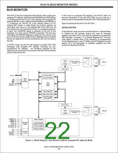
HI-6110 (BUS MONITOR MODE)
REGISTER FORMATS (MT Mode)
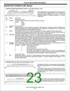
CONTROL REGISTER (R/W) Write Address: X1XX, Read Address: 1100
The Control Register value specifies HI-6110 operating mode,
clock frequency and specifies which bus is enabled for
monitoring. Control Register bits can also be used for
addressing registers in read/write operations, or to assert
master reset.
X
X
X
0
X
MSB 15 14 13 12 11 10
9
8
7
6
5
4
3
2
1
0
LSB
BIT
NAME
-
FUNCTION
Not used in MTmode.
Selects the frequency of the HI-6110 external CLK input, as follows:
15-13
12
CLKSEL
CLKSEL
Value
0
1
24 MHz
12 MHz
11
Reserved Must be reset to “0”
10 - 7 RA3:0
Register Address for HI-6110 register and data read / write operations. The register address is defined by the
logical OR of these bits and their corresponding input pins. Setting Control Register bits 10:7 to 0000 ensures
that just the address input pins control register addressing.
6
RERR
Reset ERROR. If RERR is low the ERROR output signal is only reset on reception of a new valid command.
Setting RERR high (rising edge) resets a high ERROR output . If the RERR bit is left high, ERROR outputs will
automatically reset after 3 to 4 microseconds. For normal operation, this bit is set to “1”.
5 - 4
MRB, MRA Setting either MRA or MRB to "1"connects the protocol engine to Monitor BUS A or Monitor BUS B. Setting
both MRA and MRB selects neither bus. The 1553 receiver, Manchester decoder and RCV output signal
remain operational on the inactive bus. When the monitor terminal receives a command on the inactive bus, its
RCV signal output goes high. The MT must switch active buses so received data words, message results, etc.
will be stored in the proper registers. Valid words received on the inactive bus can be read without changing
active bus by reading the BusAWord or Bus B Word Register, but any received message words, errors, message
results etc. are not updated if the bus is not enabled by setting the appropriate MRAor MRB bit.
3 - 2
RTMODE, HI-6110 mode select. These Control Register bits are logically OR'ed with their corresponding input pins. The
BCMODE user can select 1553 operating mode under either hardware or software control:
RTMODE
BCMODE 1553 OPERATING MODE
0
1
1
0
1
0
1
0
Bus Controller (BC)
RemoteTerminal (RT)
Bus Monitor without assigned RTaddress (MT)
Bus Monitor with assigned RT address (RT-MT) in which Control Register bits
5:4 enable transmit for valid commands for which command terminal address matches
the assigned RemoteTerminal address. See the RTmode section.
1
0
-
Not used in MTmode.
MR
Master Reset. Writing "1" and then “0” to this bit performs the same function as pulsing the MR pin. All register
and data FIFOs are cleared when master reset is asserted. The Control Register is the exception; it is not
affected by Master Reset.
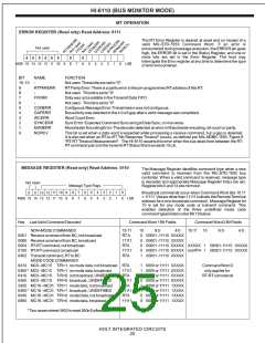
RECEIVE DATA FIFO (Read only) Read Address: 0100
MIL-STD-1553 Message Data Word 15:0
The Receive Data FIFO is 32-words deep and holds all MIL-
STD-1553 received data words. The FIFO is cleared at Master
Reset.
15 14 13 12 11 10
9
8
7
6
5
4
3
2
1
0
MSB
LSB
A low FFEMPTY flag (output pin or Status register bit) means
FIFO data is available to be read by the host. Successive data
word fetches will cause FFEMPTY to go high when the last
data word is read.
BUS A WORD REGISTER (Read only) Read Address: 1001
BUS B WORD REGISTER (Read only) Read Address: 1010
Bus A/B Word 15:0
In MT mode, the Bus A Word register holds the last valid MIL-
STD-1553 word received on Bus A. The Bus B Word register
holds the last valid MIL-STD-1553 word received on Bus B.
MSB 15 14 13 12 11 10
9
8
7
6
5
4
3
2
1
0
LSB
HOLT INTEGRATED CIRCUITS
23

 HOLTIC [ HOLT INTEGRATED CIRCUITS ]