HI-3593
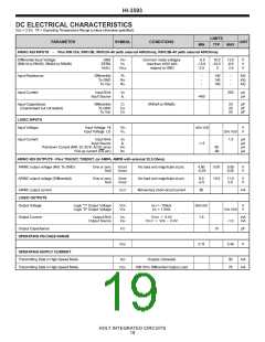
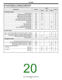
AC ELECTRICAL CHARACTERISTICS
VDD = 3.3V, TA = Operating Temperature Range and fclk=1MHz +0.1%
LIMITS
TYP
PARAMETER
SYMBOL
UNITS
MIN
MAX
SPI INTERFACE TIMING
SCK clock period
tCYC
tCHH
tCES
tCEH
tCPH
tDS
100
10
10
10
55
10
10
ns
ns
ns
ns
ns
ns
ns
ns
ns
ns
ns
ns
ns
ns
CS active after last SCK rising edge
CS setup time to first SCK rising edge
CS hold time after last SCK falling edge
CS inactive between SPI instructions
SPI SI Data set-up time to SCK rising edge
SPI SI Data hold time after SCK rising edge
SCK rise time
tDH
tSCKR
tSCKF
tSCKH
tSCKL
tDV
10
10
SCK fall ime
SCK pulse width high
20
25
SCK pulse width low
SO valid after SCK falling edge
SO high-impedance after SCK falling edge
MR pulse width
35
30
tCHZ
tMR
50
RECEIVER TIMING
Delay - Last bit of received ARINC word to Receive Flag change - Hi Speed
Delay - Last bit of received ARINC word to Receive Flag change - Lo Speed
Received data available to SPI interface. RxFLAG to CS active
SPI receiver read FIFO instruction to RxFLAG
tRFLG
tRFLG
tRXR
tSPIF
tINT
16
µs
µs
ns
ns
ns
126
0
0
tCYC
RxINT pulse width
500
TRANSMITTER TIMING
SPI transmit data write (FIFO Flag Empty or Full)
FIFO Flag delay after enable transmit instruction - Hi Speed
FIFO Flag delay to ARINC 429 data output - Hi Speed
FIFO Flag delay to ARINC 429 data output - Lo Speed
Line driver transition differential times:
tTFLG
tDATT
tSDAT
tSDAT
0
2
ns
µs
µs
µs
40
320
High Speed
high to low
low to high
high to low
low to high
tfx
trx
tfx
trx
1.0
1.0
5.0
5.0
1.5
1.5
10
2.0
2.0
15
µs
µs
µs
µs
Low Speed
10
15
HOLT INTEGRATED CIRCUITS
20

 HOLTIC [ HOLT INTEGRATED CIRCUITS ]