HT95LXXX
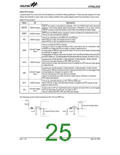
Register Label Bits R/W
Function
0~4 RO
¾
Unused bit, read as ²0²
Supported for HT95L400/40P, HT95L300/30P, HT95L100/10P, HT95L000/00P
Bit value is 0:
HT95L400/40P: SEG47~SEG44 output are available
HT95L300/30P: SEG47~SEG44 output are available
HT95L100/10P: SEG19~SEG16 output are available
SPE0
5
RW HT95L000/00P: SEG15~SEG12 output are available
Bit value is 1:
HT95L400/40P: PE3~PE0 output are available
HT95L300/30P: PE3~PE0 output are available
HT95L100/10P: PE3~PE0 output are available
HT95L000/00P: PE3~PE0 output are available
LCDIO
(28H)
Supported for HT95L400/40P, HT95L300/30P
RW Bit value is 0: SEG39~SEG36 output are available
Bit value is 1: PD3~PD0 output are available
SPD0
SPD1
6
7
Supported for HT95L400/40P, HT95L300/30P
RW Bit value is 0: SEG43~SEG40 output are available
Bit value is 1: PD7~PD4 output are available
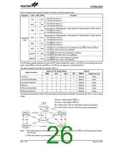
LCD Display Memory
The phone controller provides an area on embedded data memory for LCD display. The LCD display memory are lo-
cated at bank 1BH and can be read and written to, only by indirect addressing mode using MP1. When data is written
into the display data area it is automatically read by the LCD driver which then generates the corresponding LCD driv-
ing signals, to turn the display On or Off, a ²1² or ²0² is written to the corresponding bit of the display memory, respec-
tively. All of the LCD display memories are with random values after the power on reset and unchanged after other reset
conditions.
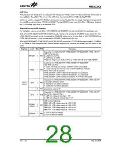
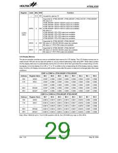
COM7 to COM0 for HT95L400/40P, HT95L300/30P
Address
40H
Register Name
SEG0
Bit 7
Bit 6
Bit 5
Bit 4
Bit 3
Bit 2
Bit 1
Bit 0
COM7
COM7
COM7
COM7
COM7
COM6
COM6
COM6
COM6
COM6
COM5
COM5
COM5
COM5
COM5
COM4
COM4
COM4
COM4
COM4
COM3
COM3
COM3
COM3
COM3
COM2
COM2
COM2
COM2
COM2
COM1
COM1
COM1
COM1
COM1
COM0
COM0
COM0
COM0
COM0
41H
SEG1
¾
¾
6EH
6FH
SEG46
SEG47
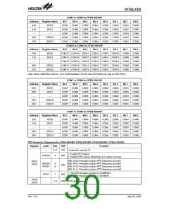
COM15 to COM8 for HT95L400/40P, HT95L300/30P
Bit 7 Bit 6 Bit 5 Bit 4 Bit 3
Address
70H
Register Name
SEG0
Bit 2
Bit 1
Bit 0
COM15 COM14 COM13 COM12 COM11 COM10 COM9
COM15 COM14 COM13 COM12 COM11 COM10 COM9
COM15 COM14 COM13 COM12 COM11 COM10 COM9
COM15 COM14 COM13 COM12 COM11 COM10 COM9
COM15 COM14 COM13 COM12 COM11 COM10 COM9
COM8
COM8
COM8
COM8
COM8
71H
SEG1
¾
¾
9EH
9FH
SEG46
SEG47
Note: When VBIAS bit set to 1 for 8 COM operation (48´8), the LCD RAM only map to (70H~9FH).
Rev. 1.20
29
May 26, 2004

 HOLTEK [ HOLTEK SEMICONDUCTOR INC ]