HT48R063/064/065/066/0662/067
¨
HT48R0662/HT48R067
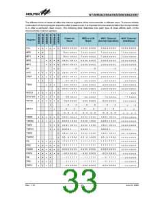
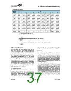
Bit
Register
POR
Name
7
6
5
4
3
2
1
0
PAWK
PAC
00H
FFH
00H
FFH
00H
FFH
00H
0FH
00H
FFH
00H
03H
00H
PAWK7 PAWK6 PAWK5 PAWK4 PAWK3 PAWK2 PAWK1 PAWK0
PAC7
¾
PAC6
PAPU6
PBC6
PBPU6
PCC6
PCPU6
PDC6
PDPU6
PEC6
PEPU6
¾
PAC5
PAPU5
PBC5
PBPU5
PCC5
PCPU5
PDC5
PDPU5
PEC5
PEPU5
¾
PAC4
PAPU4
PBC4
PBPU4
PCC4
PCPU4
PDC4
PDPU4
PEC4
PEPU4
¾
PAC3
PAPU3
PBC3
PBPU3
PCC3
PCPU3
PDC3
PDPU3
PEC3
PEPU3
¾
PAC2
PAPU2
PBC2
PBPU2
PCC2
PCPU2
PDC2
PDPU2
PEC2
PEPU2
¾
PAC1
PAPU1
PBC1
PAC0
PAPU0
PBC0
PAPU
PBC
PBC7
PBPU7
PCC7
PCPU7
PDC7
PDPU7
PEC7
PEPU7
¾
PBPU
PCC
PBPU1
PCC1
PBPU0
PCC0
PCPU
PDC
PCPU1
PDC1
PCPU0
PDC0
PDPU
PEC
PDPU1
PEC1
PDPU0
PEC0
PEPU
PFC
PEPU1
PFC1
PEPU0
PFC0
PFPU
PFPU1
PFPU0
¾
¾
¾
¾
¾
¾
²¾² Unimplemented, read as ²0²
PAWKn: PA wake-up function enable
0: disable
1: enable
PACn/PBCn/PCCn/PDCn/PECn/PFCn: I/O type selection
0: output
1: input
PAPUn/PBPUn/PCPUn/PDPUn/PEPUn/PFPUn: Pull-high function enable
0: disable
1: enable
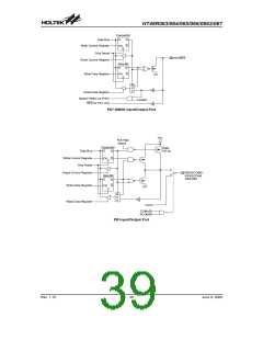
I/O Port Control Registers
multi-function I/O pins is set by configuration options
while for others the function is set by application pro-
gram control.
Each Port has its own control register, known as PAC,
PBC, PCC, PDC, PEC, PFC which controls the in-
put/output configuration. With this control register, each
I/O pin with or without pull-high resistors can be recon-
figured dynamically under software control. For the I/O
pin to function as an input, the corresponding bit of the
control register must be written as a ²1². This will then
allow the logic state of the input pin to be directly read by
instructions. When the corresponding bit of the control
register is written as a ²0², the I/O pin will be setup as a
CMOS output. If the pin is currently setup as an output,
instructions can still be used to read the output register.
However, it should be noted that the program will in fact
only read the status of the output data latch and not the
actual logic status of the output pin.
·
External Interrupt Input
The external interrupt pin, INT, is pin-shared with an
I/O pin. To use the pin as an external interrupt input
the correct bits in the INTCO register must be pro-
grammed. The pin must also be setup as an input by
setting the appropriate bit in the Port Control Register.
A pull-high resistor can also be selected via the appro-
priate port pull-high resistor register. Note that even if
the pin is setup as an external interrupt input the I/O
function still remains.
·
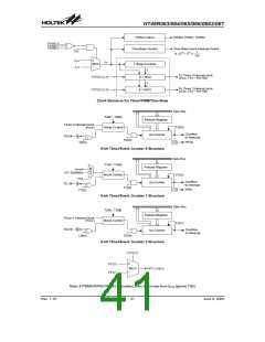
External Timer/Event Counter Input
The Timer/Event Counter pins, TC0, TC1 and TC2 are
pin-shared with I/O pins. For these shared pins to be
used as Timer/Event Counter inputs, the Timer/Event
Counter must be configured to be in the Event Coun-
ter or pulse width capture Mode. This is achieved by
setting the appropriate bits in the Timer/Event Counter
Control Register. The pins must also be setup as in-
puts by setting the appropriate bit in the Port Control
Register. Pull-high resistor options can also be se-
lected using the port pull-high resistor registers. Note
that even if the pin is setup as an external timer input
the I/O function still remains.
Pin-shared Functions
The flexibility of the microcontroller range is greatly en-
hanced by the use of pins that have more than one func-
tion. Limited numbers of pins can force serious design
constraints on designers but by supplying pins with
multi-functions, many of these difficulties can be over-
come. For some pins, the chosen function of the
Rev. 1.10
37
June 9, 2009

 HOLTEK [ HOLTEK SEMICONDUCTOR INC ]