HT48R063/064/065/066/0662/067
·
·
·
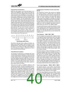
PFD Output
The PCFG bit in the CTRL0 register allows the three
function pins INT, TC0 and PFD to be remapped to dif-
ferent port pins. After power up, this bit will be reset to
zero, which will define the default port pins to which
these three functions will be mapped. Changing this bit
will move the functions to other port pins.
The device contains a PFD function whose single or
dual outputs are pin-shared with I/O pins. The output
function of these pin are chosen using the CTRL0 reg-
ister. Note that the corresponding bit of the port
control register, must setup the pin as an output to en-
able the PFD, PFD output. If the port control register
has setup these pins as input, then these pins will
function as normal logic input with the usual pull-high
selection, even if the PFD function has been selected.
Examination of the pin names on the package diagrams
will reveal that some pin function names are repeated,
this indicates a function pin that can be remapped to
other port pins. If the pin name is bracketed then this in-
dicates its alternative location. Pin names without brack-
ets indicates its default location which is the condition
after Power-on.
PWM Outputs
Some devices contain a PWM function whose outputs
are pin-shared with I/O pins. The PWM output func-
tions are chosen using the CTRL0 and CTRL2
registers. Note that the corresponding bit of the port
control registers, for the output pin, must setup the pin
as an output to enable the PWM output. If the pins are
setup as inputs, then the pin will function as a normal
logic input with the usual pull-high selections, even if
the PWM registers have enabled the PWM function.
PCFG Bit Status
PCFG Bit
0
1
INT/PA3
TC0/PA2
PFD/PA1
[INT]/PB5
[TC0]/PB4
[PFD]/PB3
Pin Mapping
SCOM Driver Pins
Pin Remapping
Pins PB0~PB3 on Port B can be used as LCD COM
driver pins. This function is controlled using the
SCOMC register which will generate the necessary
1/2 bias signals on these four pins.
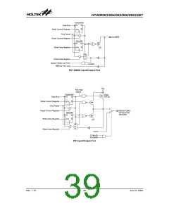
I/O Pin Structures
The diagrams illustrate the I/O pin internal structures. As
the exact logical construction of the I/O pin may differ
from these drawings, they are supplied as a guide only
to assist with the functional understanding of the I/O
pins.
Pin Remapping Configuration -
HT48R0662/HT48R067
The pin remapping function enables the function pins
INT, TC0 and PFD to be located on different port pins. It
is important not to confuse the Pin Remapping function
with the Pin-shared function, these two functions have
no interdependence.
V
D
D
P
u
l
l
-
H
i
g
h
C
o
n
t
r
o
l
B
i
t
t
S
e
l
e
c
W
e
a
k
D
a
t
a
B
u
s
D
Q
P
u
l
l
-
u
p
W
r
i
t
e
C
o
n
t
r
e
o
l
K
Q
R
e
g
i
s
t
e
r
C
S
t
C
h
i
p
R
s
e
I
/
O
p
i
n
R
e
a
d
C
o
n
t
r
o
l
R
e
g
i
s
t
e
r
D
a
t
a
B
i
t
D
C
Q
W
r
i
t
e
D
a
t
a
R
K
Q
e
g
i
s
t
e
r
S
M
U
X
R
e
a
d
D
a
t
a
R
e
g
i
s
t
e
r
P
A
o
n
l
y
S
y
s
t
e
m
W
a
k
e
-
u
p
W
a
k
e
-
u
p
S
e
l
e
c
t
Generic Input/Output Ports
Rev. 1.10
38
June 9, 2009

 HOLTEK [ HOLTEK SEMICONDUCTOR INC ]