HT48R50A-1/HT48C50-1
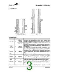
Pin Name
RES
I/O
I
Options
Description
Schmitt trigger reset input. Active low
Positive power supply
¾
¾
VDD
¾
OSC1, OSC2 are connected to an RC network or Crystal (determined by
option) for the internal system clock. In the case of RC operation, OSC2 is
the output terminal for 1/4 system clock. These two pins can also be
optioned as an RTC oscillator (32768Hz) or I/O lines. In these two cases,
the system clock comes from an internal RC oscillator whose frequency
has 4 options (3.2MHz, 1.6MHz, 800kHz, 400kHz). If the I/O option is se-
lected, the pull-high option can also be enabled or disabled. Otherwise the
PG1 and PG2 are used as internal registers (pull-high resistors are always
disabled).
Pull-high*
Crystal
or RC
OSC1/PG1
OSC2/PG2
I
O
or Int. RC+I/O
or Int. RC+RTC
Note: * The pull-high resistors of each I/O port (PA, PB, PC, PD, PG) are controlled by options.
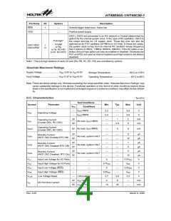
Absolute Maximum Ratings
Supply Voltage...........................VSS-0.3V to VSS+6.0V
Input Voltage..............................VSS-0.3V to VDD+0.3V
Storage Temperature............................-50°C to 125°C
Operating Temperature...........................-40°C to 85°C
Note: These are stress ratings only. Stresses exceeding the range specified under ²Absolute Maximum Ratings² may
cause substantial damage to the device. Functional operation of this device at other conditions beyond those
listed in the specification is not implied and prolonged exposure to extreme conditions may affect device reliabil-
ity.
D.C. Characteristics
Ta=25°C
Test Conditions
Conditions
Symbol
Parameter
Min.
Typ.
Max.
Unit
VDD
¾
f
SYS=4MHz
SYS=8MHz
2.2
3.3
¾
5.5
5.5
2
V
V
¾
¾
1
VDD
Operating Voltage
f
¾
3V
5V
mA
mA
Operating Current
IDD1
No load, fSYS=4MHz
No load, fSYS=8MHz
No load, system HALT
(Crystal OSC, RC OSC)
2.5
5
¾
Operating Current
IDD23
5V
4
8
mA
¾
(Crystal OSC, RC OSC)
3V
5V
3V
5V
3V
5V
¾
5
10
¾
¾
¾
¾
¾
¾
¾
¾
¾
¾
¾
¾
3.0
8
mA
mA
mA
mA
mA
mA
V
Standby Current
ISTB1
(WDT OSC Enabled RTC Off)
1
¾
Standby Current
ISTB2
No load, system HALT
No load, system HALT
(WDT OSC Disabled RTC Off)
2
¾
5
¾
Standby Current
ISTB3
(WDT OSC Disabled, RTC On)
10
¾
VIL1
VIH1
VIL2
VIH2
VLVR
0.3VDD
VDD
0.4VDD
VDD
3.3
¾
Input Low Voltage for I/O Ports
Input High Voltage for I/O Ports
Input Low Voltage (RES)
Input High Voltage (RES)
Low Voltage Reset
0
¾
0.7VDD
0
V
¾
¾
V
¾
¾
¾
0.9VDD
2.7
4
V
¾
LVRenabled
V
¾
V
OL=0.1VDD
3V
5V
mA
mA
IOL
I/O Port Sink Current
VOL=0.1VDD
10
20
¾
Rev. 2.00
4
March 8, 2006

 HOLTEK [ HOLTEK SEMICONDUCTOR INC ]