HT48R50A-1/HT48C50-1
If the stack is full and a non-masked interrupt takes
place, the interrupt request flag will be recorded but the
acknowledge signal will be inhibited. When the stack
pointer is decremented (by RET or RETI), the interrupt
will be serviced. This feature prevents stack overflow al-
lowing the programmer to use the structure more easily.
In a similar case, if the stack is full and a ²CALL² is sub-
sequently executed, stack overflow occurs and the first
entry will be lost (only the most recent 6 return ad-
dresses are stored).
I
n
d
i
r
e
c
t
A
d
d
r
e
M
s
s
i
n
g
R
e
g
i
s
t
e
r
0
0
0
0
1
H
H
P
0
I
n
d
i
r
e
c
t
A
d
d
r
e
s
s
i
n
g
R
e
g
i
s
t
e
r
1
0
2
H
M
P
1
0
3
H
0
4
H
A
C
C
0
5
H
P
C
L
0
6
H
T
B
L
P
0
7
H
T
B
L
H
0
8
H
W
D
T
S
0
9
H
S
T
A
T
U
S
0
0
A
B
H
H
I
N
T
C
Data Memory - RAM
0
0
C
D
H
H
S
p
e
c
i
a
l
P
u
r
p
o
s
e
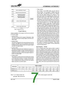
The data memory is designed with 184´8 bits. The
data memory is divided into two functional groups: spe-
cial function registers and general purpose data mem-
ory (160´8). Most are read/write, but some are read
only.
T
M
R
0
D
A
T
A
M
E
M
O
R
Y
T
T
M
M
R
R
0
1
C
H
0
E
H
0
F
H
T
M
R
1
L
1
1
0
1
H
H
T
M
R
1
C
1
2
H
P
A
The special function registers include the indirect ad-
dressing registers (00H, 02H), Timer/Event Counter 0
(TMR0;0DH), Timer/Event Counter 0 control register
(TMR0C;0EH), Timer/Event Counter 1 higher-order
byte register (TMR1H;0FH), Timer/Event Counter 1
lower-order byte register (TMR1L;10H), Timer/Event
Counter 1 control register (TMR1C;11H), Program
counter lower-order byte register (PCL;06H), Memory
pointer registers (MP0;01H, MP1;03H), Accumulator
(ACC;05H), Table pointer (TBLP;07H), Table
higher-order byte register (TBLH;08H), Status register
(STATUS;0AH), Interrupt control register (INTC;0BH),
Watchdog Timer option setting register (WDTS;09H),
I/O registers (PA;12H, PB;14H, PC;16H, PD;18H,
PG;1EH) and I/O control registers (PAC;13H,
PBC;15H, PCC;17H, PDC;19H, PGC;1FH). The re-
maining space before the 60H is reserved for future ex-
panded usage and reading these locations will get
²00H². The general purpose data memory, addressed
from 60H to FFH, is used for data and control informa-
tion under instruction commands.
1
3
H
P
A
C
1
4
H
P
B
1
5
H
P
B
C
1
6
H
P
C
1
7
H
P
C
C
1
8
H
P
D
1
9
H
P
D
C
:
U
n
u
s
e
d
1
1
A
B
H
H
R
e
a
d
a
s
"
0
0
"
1
1
C
D
H
H
1
E
H
P
G
1
F
H
P
G
C
2
0
H
5
F
H
H
6
0
G
e
n
e
r
a
l
P
u
r
p
o
s
e
D
A
T
A
M
E
M
O
R
Y
(
1
6
0
B
y
t
e
s
)
F
F
H
RAM Mapping
All of the data memory areas can handle arithmetic,
logic, increment, decrement and rotate operations di-
rectly. Except for some dedicated bits, each bit in the
data memory can be set and reset by ²SET [m].i² and
²CLR [m].i². They are also indirectly accessible through
memory pointer registers (MP0 or MP1).
Accumulator
The accumulator is closely related to ALU operations. It
is also mapped to location 05H of the data memory and
can carry out immediate data operations. The data
movement between two data memory locations must
pass through the accumulator.
Indirect Addressing Register
Arithmetic and Logic Unit - ALU
Location 00H and 02H are indirect addressing registers
that are not physically implemented. Any read/write op-
eration of [00H] ([02H]) will access data memory pointed
to by MP0 (MP1). Reading location 00H (02H) itself indi-
rectly will return the result 00H. Writing indirectly results
in no operation.
This circuit performs 8-bit arithmetic and logic operations.
The ALU provides the following functions:
·
·
·
·
·
Arithmetic operations (ADD, ADC, SUB, SBC, DAA)
Logic operations (AND, OR, XOR, CPL)
Rotation (RL, RR, RLC, RRC)
Increment and Decrement (INC, DEC)
Branch decision (SZ, SNZ, SIZ, SDZ ....)
The memory pointer registers (MP0 and MP1) are 8-bit
registers.
The ALU not only saves the results of a data operation but
also changes the status register.
Rev. 2.00
8
March 8, 2006

 HOLTEK [ HOLTEK SEMICONDUCTOR INC ]