HT48R05A-1/HT48C05/HT48R06A-1/HT48C06/HT48R08A-1
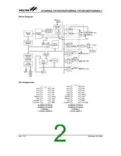
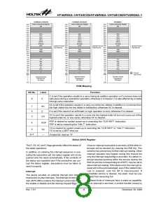
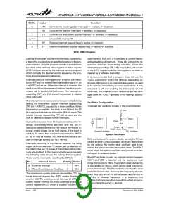
Pin Description
Pin Name
I/O
Options
Description
Bidirectional 8-bit input/output port. Each bit can be configured as wake-up
input by options. Software instructions determine the CMOS output or
Schmitt trigger input with a pull-high resistor (determined by pull-high op-
tions).
Pull-high*
Wake-up
PA0~PA7
I/O
Bidirectional 3-bit input/output port. Software instructions determine the
CMOS output or Schmitt trigger input with a pull-high resistor (determined by
pull-high options).
PB0/BZ
PB1/BZ
PB2
Pull-high*
I/O
I/O or BZ/BZ The PB0 and PB1 are pin-shared with the BZ and BZ, respectively. Once the
PB0 and PB1 are selected as buzzer driving outputs, the output signals come
from an internal PFD generator (shared with a timer/event counter).
VSS
Negative power supply, ground
¾
¾
Bidirectional I/O lines. Software instructions determine the CMOS output or
Schmitt trigger input with a pull-high resistor (determined by pull-high op-
tions). The external interrupt and timer input are pin-shared with the PC0 and
PC1, respectively. The external interrupt input is activated on a high to low
transition.
PC0/INT
I/O
Pull-high*
PC1/TMR
RES
VDD
I
Schmitt trigger reset input. Active low
Positive power supply
¾
¾
¾
OSC1, OSC2 are connected to an RC network or Crystal (determined by op-
tions) for the internal system clock. In the case of RC operation, OSC2 is the
output terminal for 1/4 system clock.
OSC1
OSC2
I
Crystal
or RC
O
* All pull-high resistors are controlled by an option bit.
Absolute Maximum Ratings
Supply Voltage...........................VSS-0.3V to VSS+6.0V
Input Voltage..............................VSS-0.3V to VDD+0.3V
Storage Temperature............................-50°C to 125°C
Operating Temperature...........................-40°C to 85°C
IOH Total............................................................-100mA
I
OL Total ..............................................................150mA
Total Power Dissipation .....................................500mW
Note: These are stress ratings only. Stresses exceeding the range specified under ²Absolute Maximum Ratings² may
cause substantial damage to the device. Functional operation of this device at other conditions beyond those
listed in the specification is not implied and prolonged exposure to extreme conditions may affect device reliabil-
ity.
D.C. Characteristics
Ta=25°C
Test Conditions
Conditions
Symbol
Parameter
Min.
Typ.
Max.
Unit
VDD
¾
fSYS=4MHz
2.2
3.3
¾
5.5
5.5
1.5
4
V
¾
¾
VDD
Operating Voltage
fSYS=8MHz
V
¾
3V
5V
3V
5V
0.6
2
mA
mA
mA
mA
IDD1
No load, fSYS=4MHz
Operating Current (Crystal OSC)
Operating Current (RC OSC)
¾
0.8
2.5
1.5
4
¾
IDD2
No load, fSYS=4MHz
No load, fSYS=8MHz
¾
Operating Current
IDD3
5V
4
8
mA
¾
(Crystal OSC, RC OSC)
Rev. 1.51
3
December 30, 2008
图片预览")
 HOLTEK [ HOLTEK SEMICONDUCTOR INC ]