HT46RU66/HT46CU66
the UCR2 register is set. The two transmitter interrupt
conditions have their own corresponding enable bits,
while the two receiver interrupt conditions have a
shared enable bit. These enable bits can be used to
mask out individual UART interrupt sources.
mode is enabled, then to ensure correct operation, the
parity function should be disabled by resetting the par-
ity enable bit to zero.
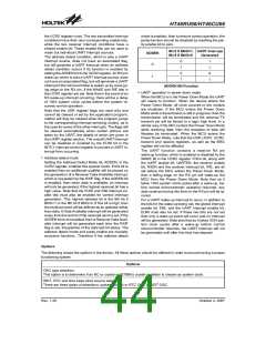
Bit 9 if BNO=1, UART Interrupt
ADDEN
Bit 8 if BNO=0
Generated
The address detect condition, which is also a UART
interrupt source, does not have an associated flag,
but will generate a UART interrupt when an address
detect condition occurs if its function is enabled by
setting the ADDEN bit in the UCR2 register. An RX pin
wake-up, which is also a UART interrupt source, does
not have an associated flag, but will generate a UART
interrupt if the microcontroller is woken up by a low go-
ing edge on the RX pin, if the WAKE and RIE bits in
the UCR2 register are set. Note that in the event of an
RX wake-up interrupt occurring, there will be a delay
of 1024 system clock cycles before the system re-
sumes normal operation.
0
1
0
1
Ö
Ö
X
Ö
0
1
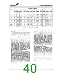
ADDEN Bit Function
·
UART operation in power down mode
When the MCU is in the Power Down Mode the UART
will cease to function. When the device enters the
Power Down Mode, all clock sources to the module
are shutdown. If the MCU enters the Power Down
Mode while a transmission is still in progress, then the
transmission will be terminated and the external TX
transmit pin will be forced to a logic high level. In a
similar way, if the MCU enters the Power Down Mode
while receiving data, then the reception of data will
likewise be terminated. When the MCU enters the
Power Down Mode, note that the USR, UCR1, UCR2,
transmit and receive registers, as well as the BRG
register will not be affected.
Note that the USR register flags are read only and
cannot be cleared or set by the application program,
neither will they be cleared when the program jumps
to the corresponding interrupt servicing routine, as is
the case for some of the other interrupts. The flags will
be cleared automatically when certain actions are
taken by the UART, the details of which are given in
the UART register section. The overall UART interrupt
can be disabled or enabled by the EURI bit in the
INTC1 interrupt control register to prevent a UART in-
terrupt from occurring.
The UART function contains a receiver RX pin
wake-up function, which is enabled or disabled by the
WAKE bit in the UCR2 register. If this bit, along with
the UART enable bit, UARTEN, the receiver enable
bit, RXEN and the receiver interrupt bit, RIE, are all
set before the MCU enters the Power Down Mode,
then a falling edge on the RX pin will wake-up the
MCU from the Power Down Mode. Note that as it
takes 1024 system clock cycles after a wake-up, be-
fore normal microcontroller operation resumes, any
data received during this time on the RX pin will be ig-
nored.
·
Address detect mode
Setting the Address Detect Mode bit, ADDEN, in the
UCR2 register, enables this special mode. If this bit is
enabled then an additional qualifier will be placed on
the generation of a Receiver Data Available interrupt,
which is requested by the RXIF flag. If the ADDEN bit
is enabled, then when data is available, an interrupt
will only be generated, if the highest received bit has a
high value. Note that the EURI and EMI interrupt en-
able bits must also be enabled for correct interrupt
generation. This highest address bit is the 9th bit if
BNO=1 or the 8th bit if BNO=0. If this bit is high, then
the received word will be defined as an address rather
than data. A Data Available interrupt will be generated
every time the last bit of the received word is set. If the
ADDEN bit is not enabled, then a Receiver Data Avail-
able interrupt will be generated each time the RXIF
flag is set, irrespective of the data last bit status. The
address detect mode and parity enable are mutually
exclusive functions. Therefore if the address detect
For a UART wake-up interrupt to occur, in addition to
the bits for the wake-up being set, the global interrupt
enable bit, EMI, and the UART interrupt enable bit,
EURI must also be set. If these two bits are not set
then only a wake up event will occur and no interrupt
will be generated. Note also that as it takes 1024 sys-
tem clock cycles after a wake-up before normal
microcontroller resumes, the UART interrupt will not
be generated until after this time has elapsed.
Options
The following shows the options in the device. All these options should be defined in order to ensure having a proper
functioning system.
Options
OSC type selection.
This option is to determine if an RC or crystal or 32768Hz crystal oscillator is chosen as system clock.
WDT, RTC and time base clock source selection.
There are three types of selections: system clock/4 or RTC OSC or WDT OSC.
Rev. 1.20
44
October 2, 2007

 HOLTEK [ HOLTEK SEMICONDUCTOR INC ]