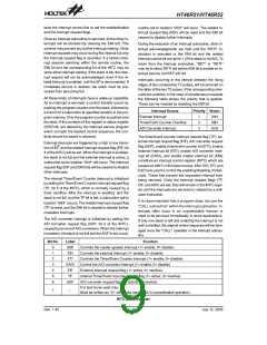
HT46R51/HT46R52
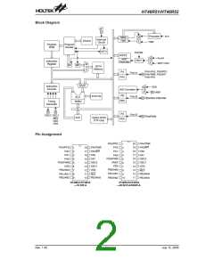
Pin Description
Pin Name I/O
Options
Description
PA0~PA2
PA3/PFD
Bidirectional 8-bit input/output port. Each individual bit on this port can be config-
ured as a wake-up input by configuration option. Software instructions determine
if the pin is a CMOS output or Schmitt trigger input. Configuration options deter-
Pull-high
Wake-up
PA4/TMR
PA5/INT
I/O
I/O
PA3 or PFD mine which pins on this port have pull-high resistors. The PFD, TMR and external
interrupt input are pin-shared with PA3, PA4, and PA5 respectively.
PA6~PA7
Bidirectional 5-bit input/output port. Software instructions determine the CMOS
output or Schmitt trigger input with or without pull-high resistor. Configuration op-
PB0/AN0
PB1/AN1
PB2/AN2
PB3/AN3
PB4/AN4
tions determine which pins on this port have pull-high resistors. PB is pin-shared
Pull-high
with the A/D input pins. The A/D inputs are selected via software instructions
Once selected as an A/D input, the I/O function and pull-high resistor functions
are disabled automatically.
Bidirectional 1-bit input/output port. Software instructions determine the CMOS
Pull-high
output or Schmitt trigger input with or without pull-high resistor. One configuration
PD0/PWM I/O
PD0 or PWM option determines which pin on this port has pull-high resistor. PD0 is pin-shared
with the PWM output selected via configuration option.
OSC1, OSC2 are connected to an external RC network or external crystal (deter-
Crystal or RC mined by configuration option) for the internal system clock. For external RC sys-
tem clock operation, OSC2 is an output pin for 1/4 system clock.
OSC1
OSC2
I
O
RES
VDD
VSS
I
Schmitt trigger reset input, active low
Positive power supply
¾
¾
¾
¾
¾
Negative power supply, ground
A/D Converter Reference Input voltage pins. Connect this pin to the desired A/D
reference voltage. The VREF pin is connected to VDD for the 18-pin DIP package
VREF
I
¾
Absolute Maximum Ratings
Supply Voltage...........................VSS-0.3V to VSS+6.0V
Input Voltage..............................VSS-0.3V to VDD+0.3V
Storage Temperature............................-50°C to 125°C
Operating Temperature...........................-40°C to 85°C
Note: These are stress ratings only. Stresses exceeding the range specified under ²Absolute Maximum Ratings² may
cause substantial damage to the device. Functional operation of this device at other conditions beyond those
listed in the specification is not implied and prolonged exposure to extreme conditions may affect device reliabil-
ity.
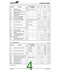
D.C. Characteristics
Ta=25°C
Test Conditions
Conditions
SYS=4MHz
Symbol
Parameter
Min.
Typ.
Max.
Unit
VDD
f
f
2.2
3.3
¾
5.5
5.5
1.5
4
V
¾
¾
VDD
Operating Voltage
¾
SYS=8MHz
V
3V
5V
3V
5V
0.6
2
mA
mA
mA
mA
No load, fSYS=4MHz
ADC disabled
IDD1
Operating Current (Crystal OSC)
¾
0.8
2.5
1.5
4
¾
No load, fSYS=4MHz
ADC disabled
IDD2
IDD3
ISTB1
Operating Current (RC OSC)
Operating Current
¾
No load, fSYS=8MHz
ADC disabled
5V
4
8
mA
¾
3V
5V
5
¾
¾
¾
¾
mA
mA
Standby Current (WDT Enabled)
No load, system HALT
10
Rev. 1.40
3
July 12, 2005

 HOLTEK [ HOLTEK SEMICONDUCTOR INC ]