HT46R064B/065B/066B
PFD Function
The residual value in the Timer/Event Counter, which
can now be read by the program, therefore represents
the length of the pulse received on the TCn pin. As the
enable bit has now been reset, any further transitions on
the external timer pin will be ignored. The timer cannot
begin further pulse width capture until the enable bit is
set high again by the program. In this way, single shot
pulse measurements can be easily made.
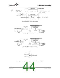
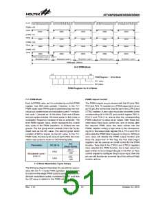
The Programmable Frequency Divider provides a
means of producing a variable frequency output suitable
for applications, such as piezo-buzzer driving or other
interfaces requiring a precise frequency generator.
The Timer/Event Counter overflow signal is the clock
source for the PFD function, which is controlled by
PFDCS bit in CTRL0. For applicable devices the clock
source can come from either Timer/Event Counter 0 or
Timer/Event Counter 1. The output frequency is con-
trolled by loading the required values into the timer
prescaler and timer registers to give the required division
ratio. The counter will begin to count-up from this preload
register value until full, at which point an overflow signal is
generated, causing both the PFD outputs to change
state. The counter will then be automatically reloaded
with the preload register value and continue counting-up.
It should be noted that in this mode the Timer/Event
Counter is controlled by logical transitions on the external
timer pin and not by the logic level. When the Timer/Event
Counter is full and overflows, an interrupt signal is gener-
ated and the Timer/Event Counter will reload the value al-
ready loaded into the preload register and continue
counting. The interrupt can be disabled by ensuring that
the Timer/Event Counter Interrupt Enable bit in the corre-
sponding Interrupt Control Register, is reset to zero.
As the TCn pin is shared with an I/O pin, to ensure that
the pin is configured to operate as a pulse width capture
pin, two things have to happen. The first is to ensure that
the Operating Mode Select bits in the Timer Control
Register place the Timer/Event Counter in the pulse
width capture Mode, the second is to ensure that the
port control register configures the pin as an input.
If the CTRL0 register has selected the PFD function,
then for PFD output to operate, it is essential for the Port
Acontrol register PAC, to setup the PFD pins as outputs.
PA1 must be set high to activate the PFD. The output
data bits can be used as the on/off control bit for the PFD
outputs. Note that the PFD outputs will all be low if the
output data bit is cleared to zero.
Using this method of frequency generation, and if a
crystal oscillator is used for the system clock, very pre-
cise values of frequency can be generated.
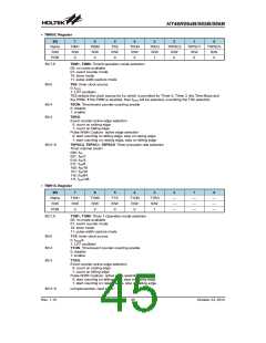
Prescaler
Bits TnPSC0~TnPSC2 of the TMRnC register can be
used to define a division ratio for the internal clock
source of the Timer/Event Counter enabling longer time
out periods to be setup.
E
x
t
e
r
n
a
l
T
C
n
P
i
n
I
n
p
u
t
T
n
O
N
-
w
i
t
h
T
n
E
=
0
P
r
e
s
c
a
l
e
r
O
u
t
p
u
t
I
n
c
r
e
m
e
n
t
+
1
+
2
+
3
+
4
T
i
m
e
r
T
i
m
e
r
C
o
u
n
t
e
r
P
r
e
s
c
a
l
e
r
O
u
t
p
u
t
i
s
s
a
m
p
l
e
d
a
t
e
v
e
r
y
f
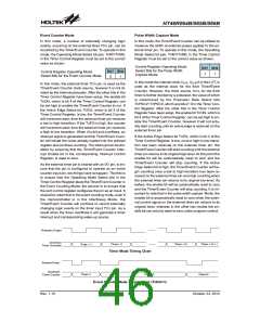
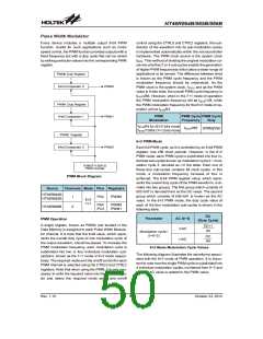
Pulse Width Capture Mode Timing Chart (TnE=0)
T
i
m
e
r
O
v
e
r
f
l
o
w
P
F
D
C
l
o
c
k
P
A
1
D
a
t
a
P
F
D
O
u
t
p
u
t
a
t
P
A
1
PFD Function
Rev. 1.10
47
October 23, 2012

 HOLTEK [ HOLTEK SEMICONDUCTOR INC ]