HT46R064B/065B/066B
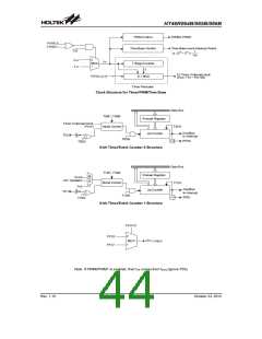
Configuring the Timer/Event Counter Input Clock
Source
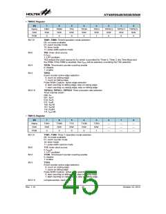
The Timer Control Register is known as TMRnC. It is the
Timer Control Register together with its corresponding
timer register that control the full operation of the
Timer/Event Counter. Before the timer can be used, it is
essential that the Timer Control Register is fully pro-
grammed with the right data to ensure its correct opera-
tion, a process that is normally carried out during
program initialisation.
The Timer/Event Counter clock source can originate
from various sources, an internal clock or an external
pin. The internal clock source source is used when the
timer is in the timer mode or in the pulse width capture
mode. For some Timer/Event Counters, this internal
clock source is first divided by a prescaler, the division
ratio of which is conditioned by the Timer Control Regis-
ter bits T0PSC0~T0PSC2. For Timer/Event Counter 0,
the internal clock source can be either fSYS or the LXT
Oscillator, the choice of which is determined by the T0S
bit in the TMR0C register.
To choose which of the three modes the timer is to oper-
ate in, either in the timer mode, the event counting mode
or the pulse width capture mode, bits 7 and 6 of the
Timer Control Register, which are known as the bit pair
TnM1/TnM0, must be set to the required logic levels.
The timer-on bit, which is bit 4 of the Timer Control Reg-
ister and known as TnON, provides the basic on/off con-
trol of the respective timer. Setting the bit high allows the
counter to run, clearing the bit stops the counter. Bits
0~2 of the Timer Control Register determine the division
ratio of the input clock prescaler. The prescaler bit set-
tings have no effect if an external clock source is used. If
the timer is in the event count or pulse width capture
mode, the active transition edge level type is selected by
the logic level of bit 3 of the Timer Control Register
which is known as TnEG. The TnS bit selects the inter-
nal clock source if used.
An external clock source is used when the timer is in the
event counting mode, the clock source being provided
on an external timer pin TCn. Depending upon the con-
dition of the TnEG bit, each high to low, or low to high
transition on the external timer pin will increment the
counter by one.
Timer Registers - TMR0, TMR1
The timer registers are special function registers located
in the Special Purpose Data Memory and is the place
where the actual timer value is stored. These registers
are known as TMR0 and TMR1. The value in the timer
registers increases by one each time an internal clock
pulse is received or an external transition occurs on the
external timer pin. The timer will count from the initial
value loaded by the preload register to the full count of
FFH at which point the timer overflows and an internal
interrupt signal is generated. The timer value will then
be reset with the initial preload register value and con-
tinue counting.
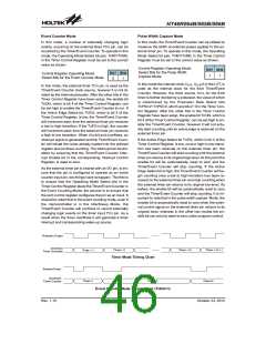
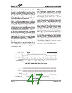
Timer Mode
In this mode, the Timer/Event Counter can be utilised to
measure fixed time intervals, providing an internal inter-
rupt signal each time the Timer/Event Counter over-
flows. To operate in this mode, the Operating Mode
Select bit pair, TnM1/TnM0, in the Timer Control Regis-
ter must be set to the correct value as shown.
Note that to achieve a maximum full range count of FFH,
the preload register must first be cleared to all zeros. It
should be noted that after power-on, the preload regis-
ters will be in an unknown condition. Note that if the
Timer/Event Counter is in an OFF condition and data is
written to its preload register, this data will be immedi-
ately written into the actual counter. However, if the
counter is enabled and counting, any new data written
into the preload data register during this period will re-
main in the preload register and will only be written into
the actual counter the next time an overflow occurs.
Bit7 Bit6
Control Register Operating Mode
Select Bits for the Timer Mode
1
0
In this mode the internal clock is used as the timer clock.
The timer input clock source is either fSYS , fSYS/4 or the
LXT oscillator. However, this timer clock source is fur-
ther divided by a prescaler, the value of which is deter-
mined by the bits TnPSC2~TnPSC0 in the Timer
Control Register. The timer-on bit, TnON must be set
high to enable the timer to run. Each time an internal
clock high to low transition occurs, the timer increments
by one; when the timer is full and overflows, an interrupt
signal is generated and the timer will reload the value al-
ready loaded into the preload register and continue
counting. A timer overflow condition and corresponding
internal interrupt is one of the wake-up sources, how-
ever, the internal interrupts can be disabled by ensuring
that the ETnI bits of the INTCn register are reset to zero.
Timer Control Registers - TMR0C, TMR1C
The flexible features of the Holtek microcontroller
Timer/Event Counters enable them to operate in three
different modes, the options of which are determined by
the contents of their respective control register.
Rev. 1.10
43
October 23, 2012

 HOLTEK [ HOLTEK SEMICONDUCTOR INC ]