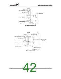
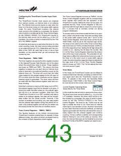
HT46R064B/065B/066B
Event Counter Mode
Pulse Width Capture Mode
In this mode, a number of externally changing logic
events, occurring on the external timer TCn pin, can be
recorded by the Timer/Event Counter. To operate in this
mode, the Operating Mode Select bit pair, TnM1/TnM0,
in the Timer Control Register must be set to the correct
value as shown.
In this mode, the Timer/Event Counter can be utilised to
measure the width of external pulses applied to the ex-
ternal timer pin. To operate in this mode, the Operating
Mode Select bit pair, TnM1/TnM0, in the Timer Control
Register must be set to the correct value as shown.
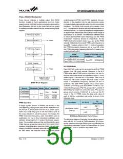
Control Register Operating Mode
Bit7 Bit6
Select Bits for the Pulse Width
Bit7 Bit6
Control Register Operating Mode
1
1
Capture Mode
Select Bits for the Event Counter Mode
0
1
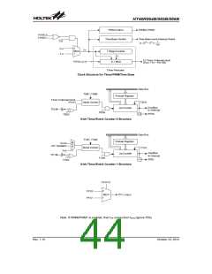
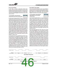
In this mode the internal clock, fSYS , fSYS/4 or the LXT, is
used as the internal clock for the 8-bit Timer/Event
Counter. However, the clock source, fSYS, for the 8-bit
timer is further divided by a prescaler, the value of which
is determined by the Prescaler Rate Select bits
TnPSC2~TnPSC0, which are bits 2~0 in the Timer Con-
trol Register. After the other bits in the Timer Control
Register have been setup, the enable bit TnON, which is
bit 4 of the Timer Control Register, can be set high to en-
able the Timer/Event Counter, however it will not actu-
ally start counting until an active edge is received on the
external timer pin.
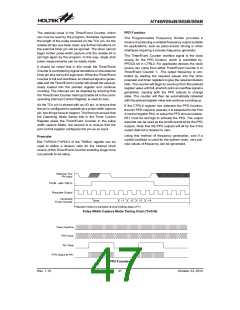
In this mode, the external timer TCn pin, is used as the
Timer/Event Counter clock source, however it is not di-
vided by the internal prescaler. After the other bits in the
Timer Control Register have been setup, the enable bit
TnON, which is bit 4 of the Timer Control Register, can
be set high to enable the Timer/Event Counter to run. If
the Active Edge Select bit, TnEG, which is bit 3 of the
Timer Control Register, is low, the Timer/Event Counter
will increment each time the external timer pin receives
a low to high transition. If the TnEG is high, the counter
will increment each time the external timer pin receives
a high to low transition. When it is full and overflows, an
interrupt signal is generated and the Timer/Event Coun-
ter will reload the value already loaded into the preload
register and continue counting. The interrupt can be dis-
abled by ensuring that the Timer/Event Counter Inter-
rupt Enable bit in the corresponding Interrupt Control
Register, is reset to zero.
If the Active Edge Select bit TnEG, which is bit 3 of the
Timer Control Register, is low, once a high to low transi-
tion has been received on the external timer pin, the
Timer/Event Counter will start counting until the external
timer pin returns to its original high level. At this point the
enable bit will be automatically reset to zero and the
Timer/Event Counter will stop counting. If the Active
Edge Select bit is high, the Timer/Event Counter will be-
gin counting once a low to high transition has been re-
ceived on the external timer pin and stop counting when
the external timer pin returns to its original low level. As
before, the enable bit will be automatically reset to zero
and the Timer/Event Counter will stop counting. It is im-
portant to note that in the pulse width capture Mode, the
enable bit is automatically reset to zero when the exter-
nal control signal on the external timer pin returns to its
original level, whereas in the other two modes the en-
able bit can only be reset to zero under program control.
As the external timer pin is shared with an I/O pin, to en-
sure that the pin is configured to operate as an event
counter input pin, two things have to happen. The first is
to ensure that the Operating Mode Select bits in the
Timer Control Register place the Timer/Event Counter in
the Event Counting Mode, the second is to ensure that
the port control register configures the pin as an input. It
should be noted that in the event counting mode, even if
the microcontroller is in the Idle/Sleep Mode, the
Timer/Event Counter will continue to record externally
changing logic events on the timer input TCn pin. As a
result when the timer overflows it will generate a timer
interrupt and corresponding wake-up source.
P
r
e
s
c
a
l
e
r
O
u
t
p
u
t
I
n
c
r
e
m
e
n
t
T
i
m
e
r
+
2
T
i
m
e
r
+
T
N
i
m
e
r
T
i
m
e r
r
+
1
T
i
m
e
r
C
o
n
t
r
o
l
l
e
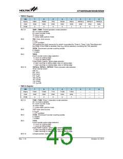
Timer Mode Timing Chart
E
x
t
e
r
n
a
l
E
v
e
n
t
I
n
c
r
e
m
e
n
t
T
i m
r
e
r
+
1
T
i
m
e
r
+
2
T
i
m
e
r
+
T
i
m
e
r
C
o
u
n
t
e
Event Counter Mode Timing Chart (TnEG=1)
Rev. 1.10
46
October 23, 2012

 HOLTEK [ HOLTEK SEMICONDUCTOR INC ]