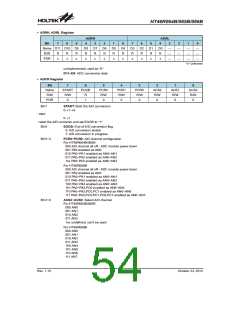
HT46R064B/065B/066B
Pulse Width Modulator
Every device includes a multiple output 8-bit PWM
function. Useful for such applications such as motor
speed control, the PWM function provides outputs with a
fixed frequency but with a duty cycle that can be varied
by setting particular values into the corresponding PWM
register.
control using the CTRL0 and CTRL2 registers, the sub-
division of the waveform into its sub-modulation cycles
is implemented automatically within the microcontroller
hardware. The PWM clock source is the system clock
fSYS. This method of dividing the original modulation cy-
cle into a further 2 or 4 sub-cycles enable the generation
of higher PWM frequencies which allow a wider range of
applications to be served. The difference between what
is known as the PWM cycle frequency and the PWM
modulation frequency should be understood. As the
PWM clock is the system clock, fSYS, and as the PWM
value is 8-bits wide, the overall PWM cycle frequency is
P
W
M
0
D
u
t
y
R
e
g
i
s
t
e
r
8
-
b
i
t
C
o
m
p
a
r
P
a
M
t
o
W
r
0
0
f
SYS/256. However, when in the 7+1 mode of operation
the PWM modulation frequency will be fSYS/128, while
the PWM modulation frequency for the 6+2 mode of op-
eration will be fSYS/64.
P
W
M
1
D
u
t
y
R
e
g
i
s
t
e
r
PWM
PWM Cycle PWM Cycle
8
-
b
i
t
C
o
m
p
a
r
P
a
M
t
o
W
r
1
1
Modulation
Frequency
Duty
f
SYS/64 for (6+2) bits mode
SYS/128for (7+1) bits mode
f
SYS/256
[PWM]/256
f
P
W
M
2
R
e
g
i
s
t
e
r
6+2 PWM Mode
8
-
b
i
t
C
o
m
p
a
r
P
a
M
t
o
W
r
2
2
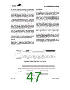
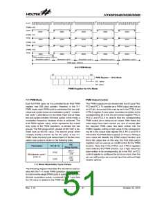
Each full PWM cycle, as it is controlled by an 8-bit PWM
register, has 256 clock periods. However, in the 6+2
PWM mode, each PWM cycle is subdivided into four in-
dividual sub-cycles known as modulation cycle 0 ~ mod-
ulation cycle 3, denoted as i in the table. Each one of
these four sub-cycles contains 64 clock cycles. In this
mode, a modulation frequency increase of four is
achieved. The 8-bit PWM register value, which repre-
sents the overall duty cycle of the PWM waveform, is di-
vided into two groups. The first group which consists of
bit2~bit7 is denoted here as the DC value. The second
group which consists of bit0~bit1 is known as the AC
value. In the 6+2 PWM mode, the duty cycle value of
each of the four modulation sub-cycles is shown in the
following table.
8
-
b
i
t
/
(
7
+
1
)
/
P
W
M
C
o
u
n
t
e
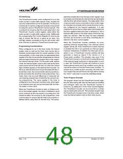
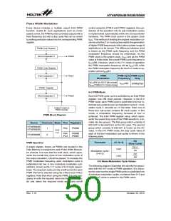
PWM Block Diagram
Device
Channels Mode Pins Registers
HT46R064B
HT46R065B
1
2
PA4
PWM0
6+2
7+1
PA4
PC3
PWM0
PWM1
HT46R066B
DC
Parameter
AC (0~3)
i<AC
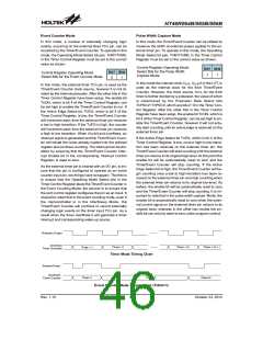
PWM Operation
(Duty Cycle)
A single register, known as PWMn and located in the
Data Memory is assigned to each Pulse Width Modula-
tor channel. It is here that the 8-bit value, which repre-
sents the overall duty cycle of one modulation cycle of
the output waveform, should be placed. To increase the
PWM modulation frequency, each modulation cycle is
subdivided into two or four individual modulation sub-
sections, known as the 7+1 mode or 6+2 mode respec-
tively. The required mode and the on/off control for each
PWM channel is selected using the CTRL0 and CTRL2
registers. Note that when using the PWM, it is only nec-
essary to write the required value into the PWMn regis-
ter and select the required mode setup and on/off
DC+1
64
Modulation cycle i
(i=0~3)
DC
64
i³AC
6+2 Mode Modulation Cycle Values
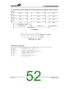
The following diagram illustrates the waveforms associ-
ated with the 6+2 mode of PWM operation. It is impor-
tant to note how the single PWM cycle is subdivided into
4 individual modulation cycles, numbered from 0~3 and
how the AC value is related to the PWM value.
Rev. 1.10
50
October 23, 2012

 HOLTEK [ HOLTEK SEMICONDUCTOR INC ]