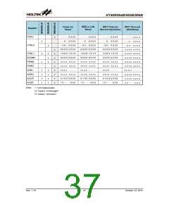
HT46R064B/065B/066B
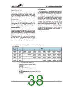
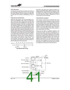
I/O Pin Structures
Pins PA0 to PA7 each have a wake-up functions, se-
lected via the PAWK register. When the device is in the
Idle/Sleep Mode, various methods are available to wake
the device up. One of these is a high to low transition of
any of the these pins. Single or multiple pins on Port A
can be setup to have this function.
The diagrams illustrate the I/O pin internal structures. As
the exact logical construction of the I/O pin may differ
from these drawings, they are supplied as a guide only
to assist with the functional understanding of the I/O
pins.
Programming Considerations
Timer/Event Counters
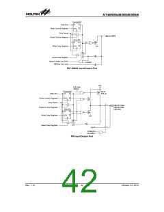
Within the user program, one of the first things to con-
sider is port initialisation. After a reset, the I/O data reg-
ister and I/O port control register will be set high. This
means that all I/O pins will default to an input state, the
level of which depends on the other connected circuitry
and whether pull-high options have been selected. If the
port control registers, are then programmed to setup
some pins as outputs, these output pins will have an ini-
tial high output value unless the associated port data
register is first programmed. Selecting which pins are in-
puts and which are outputs can be achieved byte-wide
by loading the correct value into the port control register
or by programming individual bits in the port control reg-
ister using the ²SET [m].i² and ²CLR [m].i² instructions.
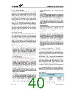
Note that when using these bit control instructions, a
read-modify-write operation takes place. The
microcontroller must first read in the data on the entire
port, modify it to the required new bit values and then re-
write this data back to the output ports.
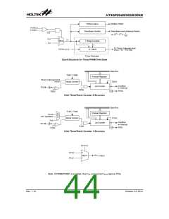
The provision of timers form an important part of any
microcontroller, giving the designer a means of carrying
out time related functions. The devices contain from one
to three count-up timer of 8-bit capacity. As the timers
have three different operating modes, they can be con-
figured to operate as a general timer, an external event
counter or as a pulse width capture device. The provi-
sion of an internal prescaler to the clock circuitry on
gives added range to the timers.
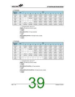
There are two types of registers related to the
Timer/Event Counters. The first is the register that con-
tains the actual value of the timer and into which an ini-
tial value can be preloaded. Reading from this register
retrieves the contents of the Timer/Event Counter. The
second type of associated register is the Timer Control
Register which defines the timer options and deter-
mines how the timer is to be used. The device can have
the timer clock configured to come from the internal
clock source. In addition, the timer clock source can also
be configured to come from an external timer pin.
T
1
T
2
T
3
T
4
T
1
T
2
T
3
T
4
S
y
s
t
e
m
C
l
o
c
k
P
o
r
t
D
a
t
a
R
e
a
d
f
r
o
m
P
W
o
r
r
i
t
t
e
t
o
P
o
r
t
Read Modify Write Timing
V
D
D
P
u
l
l
-
H
i
g
h
C
o
n
t
r
o
l
B
i
t
t
S
e
l
e
c
W
e
a
k
D
a
t
a
B
u
s
D
Q
P
u
l
l
-
u
p
W
r
i
t
e
C
o
n
t
r
e
o
l
K
Q
R
e
g
i
s
t
e
r
C
S
t
C
h
i
p
R
s
e
I
/
O
p
i
n
R
e
a
d
C
o
n
t
r
o
l
R
e
g
i
s
t
e
r
D
a
t
a
B
i
t
D
C
Q
W
r
i
t
e
D
a
t
a
R
K
Q
e
g
i
s
t
e
r
S
M
U
X
R
e
a
d
D
a
t
a
R
e
g
i
s
t
e
r
P
A
o
n
l
y
S
y
s
t
e
m
W
a
k
e
-
u
p
W
a
k
e
-
u
p
S
e
l
e
c
t
Generic Input/Output Ports
Rev. 1.10
41
October 23, 2012

 HOLTEK [ HOLTEK SEMICONDUCTOR INC ]