HT46F46E/HT46F47E/HT46F48E/HT46F49E
0
0
H
0
0
H
0
0
H
S
D
p
e
c
i
a
l
P
u
r
p
o
s
e
S
D
p
e
c
i
a
l
P
u
r
p
o
s
e
S
D
p
e
c
i
a
l
a
t
a
M
e
m
o
r
y
a
t
a
M
e
m
o
r
y
a
t
a
M
e
2
2
7
8
H
H
3
F
H
H
3
F
H
H
4
0
4
0
G
D
e
n
e
r
a
l
P
u
r
p
o
s
e
G
D
e
n
e
r
a
l
P
u
r
p
o
s
e
a
t
a
M
e
m
o
r
y
a
t
a
M
e
m
o
r
y
G
D
e
n
e
r
a
l
a
t
a
M
e
7
F
H
7
F
H
H
T
4
6
F
4
6
E
a
n
d
H
T
4
6
F
4
7
H
E
T
4
6
F
4
8
E
B
F
H
H
T
4
6
F
4
9
E
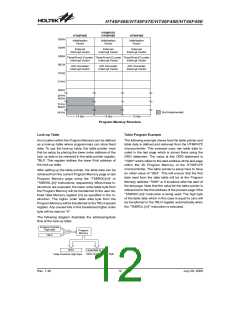
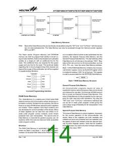
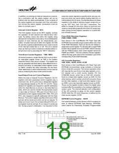
Data Memory Structure
Note:
Most of the Data Memory bits can be directly manipulated using the ²SET [m].i² and ²CLR [m].i² with the excep-
tion of a few dedicated bits. The Data Memory can also be accessed through the memory pointer registers
MP0 and MP1.
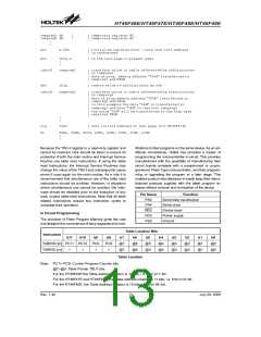
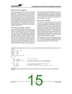
The Flash device Program Memory and EEPROM
memory can both be programmed serially in-circuit us-
ing a 5-wire interface. Data is downloaded and uploaded
serially on a single pin with an additional line for the
clock. Two additional lines are required for the power
supply and one line for the reset. The technical details
regarding the in-circuit programming of the devices are
beyond the scope of this publication but will be supplied
in supplementary literature.
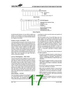
ory is located in Bank 0 which is also subdivided into two
sections, the Special Purpose Data Memory and the
General Purpose Data Memory. The start address of the
Data Memory for all devices is the address ²00H². Reg-
isters which are common to all microcontrollers, such as
ACC, PCL, etc., have the same Data Memory address.
Bank 1 of the RAM Data Memory contains only one spe-
cial function register, known as the EECR register which
is located at address ²40H² for all devices. This register
is used to access data from the EEPROM Data Memory.
C
o
n
n
e
c
t
o
r
P
o
w
e
r
V
V
P
P
R
D
S
A
A
D
4
0
H
E
E
C
R
G
r
o
u
n
d
S
0
4
Bank 1 RAM Data Memory Structure
D
a
t
a
C
l
o
c
k
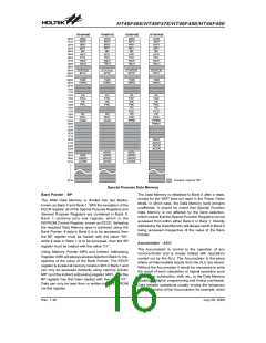
General Purpose Data Memory
R
e
s
e
t
E
S
All microcontroller programs require an area of
read/write memory where temporary data can be stored
and retrieved for use later. It is this area of RAM memory
that is known as General Purpose Data Memory. This
area of Data Memory is fully accessible by the user pro-
gram for both read and write operations. By using the
²SET [m].i² and ²CLR [m].i² instructions individual bits
can be set or reset under program control giving the
user a large range of flexibility for bit manipulation in the
Data Memory.
In-circuit Programming Interface
RAM Data Memory
The Data Memory is a volatile area of 8-bit wide RAM
internal memory and is the location where temporary in-
formation is stored. Divided into two sections, the first of
these is an area of RAM where special function registers
are located. These registers have fixed locations and
are necessary for correct operation of the device. Many
of these registers can be read from and written to di-
rectly under program control, however, some remain
protected from user manipulation. The second area of
Data Memory is reserved for general purpose use. All
locations within this area are read and write accessible
under program control.
Special Purpose Data Memory
This area of Data Memory is where registers, necessary
for the correct operation of the microcontroller, are
stored. Most of the registers are both readable and
writable but some are protected and are readable only,
the details of which are located under the relevant Spe-
cial Function Register section. Note that for locations
that are unused, any read instruction to these addresses
will return the value ²00H².
Structure
The RAM Data Memory is subdivided into two banks,
known as Bank 0 and Bank 1, all of which are imple-
mented in 8-bit wide RAM. Most of the RAM Data Mem-
Rev. 1.40
14
July 28, 2009

 HOLTEK [ HOLTEK SEMICONDUCTOR INC ]