HT46RU25/HT46CU25
Pin Description
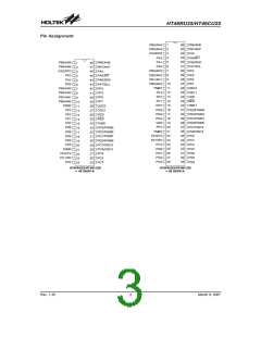
Pin Name
I/O
Options
Description
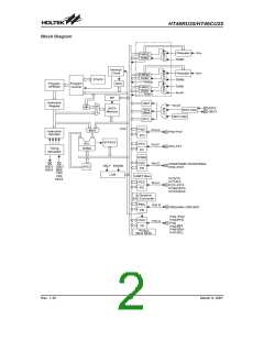
PA0~PA2
PA3/PFD
PA4
Bidirectional 8-bit input/output port. Each bit can be configured as wake-up
input by option (bit option). Software instructions determine the CMOS out-
put or Schmitt trigger input with or without pull-high resistor (determine by
Pull-high
Wake-up
I/O
PA5/INT
PA6/SDA
PA7/SCL
PA3 or PFD pull-high options: bit option). The PFD and INT are pin-shared with PA3
I/O or I2C Bus and PA5, respectively. Once the I2C Bus function is used, the internal reg-
isters related to PA6 and PA7 cannot be used.
Bidirectional 8-bit input/output port. Software instructions determine the
CMOS output, Schmitt trigger input with or without pull-high resistor (deter-
PB0/AN0~
PB7/AN7
I/O
Pull-high
mined by pull-high option: bit option) or A/D input. Once a PB line is se-
lected as an A/D input (by using software control), the I/O function and
pull-high resistor are automatically disabled.
Bidirectional 8-bit input/output port. Software instructions determine the
CMOS output, Schmitt trigger input with or without pull-high resistor (deter-
mine by pull-high option: byte option).
PC0/TX
PC1/RX
Pull-high
TX and RX are pin-shared with PC0 and PC1, once the UART Bus function
is used, the internal registers related to PC0 and PC1 cannot be used.
Software instructions determine the UART function to be used.
OSC3/OSC4 are pin shared with PC6/PC7. (depending on the OSC type
option)
PC2~PC5
PC6/OSC3
PC7/OSC4
I/O I/O or UART
OSC3/OSC4
PD0/PWM0
PD1/PWM1
PD2/PWM2
PD3/PWM3
PD4~PD7
Bidirectional 8-bit input/output port. Software instructions determine the
CMOS output, Schmitt trigger input with or without a pull-high resistor (de-
termined by pull-high option: byte option). The PWM0/PWM1/PWM2/
PWM3 output function are pin-shared with PD0/PD1/PD2/PD3 (depending
on the PWM options).
Pull-high
I/O
PWM
Bidirectional 8-bit input/output port. Software instructions determine the
CMOS output, Schmitt trigger input with or without pull-high resistor (deter-
mine by pull-high option: byte option).
PF0~PF7
I/O
I/O
Pull-high
Pull-high
Bidirectional 8-bit input/output port. Software instructions determine the
CMOS output, Schmitt trigger input with or without pull-high resistor (deter-
mine by pull-high option: byte option).
PG0~PG7
(56-pin package only)
TMR0
TMR1
TMR2
RES
I
I
Timer/Event Counter 0 Schmitt trigger input (without pull-high resistor)
Timer/Event Counter 1 Schmitt trigger input (without pull-high resistor).
Timer/Event Counter 2 Schmitt trigger input (without pull-high resistor).
Schmitt trigger reset input, active low
¾
¾
¾
¾
¾
¾
I
I
VSS
Negative power supply, ground
¾
¾
VDD
Positive power supply
OSC1 and OSC2 are connected to an RC network or a crystal (by options)
for the internal system clock. In the case of RC operation, OSC2 is the
output terminal for 1/4 system clock.
OSC1
OSC2
I
Crystal
or RC
O
Absolute Maximum Ratings
Supply Voltage...........................VSS-0.3V to VSS+6.0V
Input Voltage..............................VSS-0.3V to VDD+0.3V
Storage Temperature............................-50°C to 125°C
Operating Temperature...........................-40°C to 85°C
IOH Total............................................................-100mA
I
OL Total ..............................................................150mA
Total Power Dissipation .....................................500mW
Note: These are stress ratings only. Stresses exceeding the range specified under ²Absolute Maximum Ratings² may
cause substantial damage to the device. Functional operation of this device at other conditions beyond those
listed in the specification is not implied and prolonged exposure to extreme conditions may affect device
reliability.
Rev. 1.30
4
March 9, 2007

 HOLTEK [ HOLTEK SEMICONDUCTOR INC ]