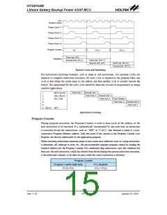
HT45FH4M
Lithium Battery Backup Power ASSP MCU
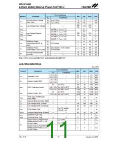
Test Conditions
Symbol
Parameter
Min.
Typ.
Max. Unit
VDD
Conditions
Sꢂstem Reset Delaꢂ Time
(Poweꢁ On Reset)
—
—
ꢅꢃ
ꢃ0
100
ms
ms
tRSTD
Sꢂstem Reset Delaꢂ Time
(Anꢂ Reset except Poweꢁ On
Reset)
—
—
8.ꢆ
16.7
ꢆꢆ.ꢆ
Note:ꢀ1.ꢀtSYS=ꢀ1/fSYS;ꢀ SUBꢀ=ꢀ1/fSUB
t
2.ꢀToꢀmaintainꢀtheꢀaccuracyꢀofꢀtheꢀinternalꢀHIRCꢀoscillatorꢀfrequency,ꢀaꢀ0.1μFꢀdecouplingꢀcapacitorꢀshouldꢀ
beꢀconnectedꢀbetweenꢀVDDꢀandꢀVSSꢀandꢀlocatedꢀasꢀcloseꢀtoꢀtheꢀdeviceꢀasꢀpossible.
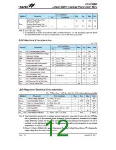
ADC Electrical Characteristics
Ta=ꢀ25°C
Test Conditions
Symbol
Parameter
Min. Typ. Max. Unit
VDD
—
Conditions
VADI
VREF
VBG
A/D Conveꢁteꢁ Inpꢀt Voltage
A/D Conveꢁteꢁ Refeꢁence Voltage
Refeꢁence Voltage
—
—
—
0
ꢅ
—
—
VREF
VDD
V
V
—
—
-ꢆ%
—
—
—
—
1.ꢅꢃ +ꢆ%
V
DNL
INL
Diffeꢁential Non-lineaꢁitꢂ
Integꢁal Non-lineaꢁitꢂ
ꢃV tADCK= 1.0μs
±1
±ꢅ
±ꢅ
±4
LSB
LSB
mA
mA
ꢃV tADCK= 1.0μs
ꢆV No load (tADCK= 0.5μs )
ꢃV No load (tADCK= 0.5μs )
0.9
1.ꢅ
1.ꢆꢃ
1.8
Additional Poweꢁ Consꢀmption
if A/D Conveꢁteꢁ is ꢀsed
IADC
Additional Poweꢁ Consꢀmption
if VBG Refeꢁence with Bꢀffeꢁ is ꢀsed
IBG
—
—
—
—
—
—
0.ꢃ
—
ꢅ00
—
ꢆ00
10
μA
μs
tADCK
tADC
A/D Conveꢁteꢁ Clock Peꢁiod
A/D Conveꢁsion Time
(Inclꢀde Sample and Hold Time)
1ꢅ bit ADC
16
—
tADCK
tADS
A/D Conveꢁteꢁ Sampling Time
A/D Conveꢁteꢁ On-to-Staꢁt Time
VBG Tꢀꢁn on Stable Time
—
—
—
—
—
—
—
ꢅ
4
—
—
—
tADCK
μs
tONꢅST
tBGS
—
—
ꢅ00
μs
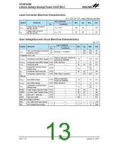
LDO Regulator Electrical Characteristics
V5=ꢀ5V,ꢀVIN=ꢀVOUTꢀ+ꢀ1.0V,ꢀIO=ꢀ1mA,ꢀTa=ꢀ25°C,ꢀunlessꢀotherwiseꢀspecified
Symbol
ΔVOUT
ΔVLOAD
VDROP
ISS
Parameter
Oꢀtpꢀt Voltage Toleꢁance
Load Regꢀlation (Note 1)
Dꢁop Oꢀt Voltage (Note ꢅ)
Qꢀienscent Cꢀꢁꢁent
Line Regꢀlation
Test Conditions
IO=10mAꢄ Ta= ꢅꢃ°C
Min.
-ꢅ
Typ.
—
Max.
ꢅ
Unit
%/V
%/mA
mV
1mA≤ IO≤ 30mA
IO= 1mAꢄ ΔVO= ꢅ%
IO= 0mA
—
0.09
—
0.18
100
4
—
—
ꢅ
μA
ΔVLINE
VIN
1.0V+ΔVOUT≤ VIN≤ 28V, IO= 1mA
—
—
0.ꢅ
—
—
%/V
V
Inpꢀt Voltage VCC
—
ꢅ8
ΔVOUT/ΔTa Temperature Coefficient
IO= 10mAꢄ -40°C< Ta< 8ꢃ°C
—
±0.9
—
mV/°C
Note:ꢀ1.ꢀLoadꢀregulationꢀisꢀmeasuredꢀatꢀaꢀconstantꢀjunctionꢀtemperature,ꢀusingꢀpulseꢀtestingꢀwithꢀaꢀlowꢀONꢀtimeꢀ
andꢀisꢀguaranteedꢀupꢀtoꢀtheꢀmaximumꢀpowerꢀdissipation.ꢀPowerꢀdissipationꢀisꢀdeterminedꢀbyꢀtheꢀinput/
outputꢀdifferentialꢀvoltageꢀandꢀtheꢀoutputꢀcurrent.ꢀGuaranteedꢀmaximumꢀpowerꢀdissipationꢀwillꢀnotꢀbeꢀ
availableꢀoverꢀtheꢀfullꢀinput/outputꢀrange.ꢀTheꢀmaximumꢀallowableꢀpowerꢀdissipationꢀatꢀanyꢀambientꢀ
temperatureꢀisꢀPDꢀ=ꢀ(TJ(MAX)-Ta)/θJA.
2.ꢀDropoutꢀvoltageꢀisꢀdefinedꢀasꢀtheꢀinputꢀvoltageꢀminusꢀtheꢀoutputꢀvoltageꢀthatꢀproducesꢀaꢀ2%ꢀchangeꢀinꢀtheꢀ
outputꢀvoltageꢀfromꢀtheꢀvalueꢀatꢀVIN=ꢀVOUT+2V.
Rev. 1.10
1ꢅ
�anꢀaꢁꢂ 1ꢃꢄ ꢅ01ꢆ

 HOLTEK [ HOLTEK SEMICONDUCTOR INC ]