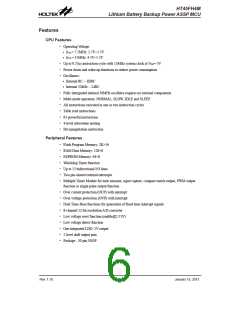
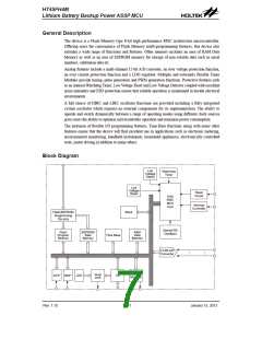
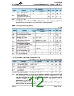
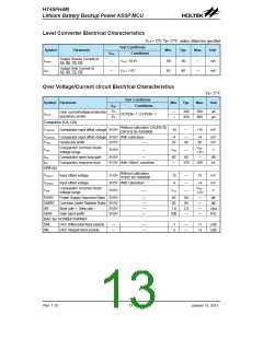
HT45FH4M
Lithium Battery Backup Power ASSP MCU
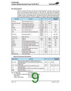
Pin Description
Withꢀtheꢀexceptionꢀofꢀtheꢀpowerꢀpinsꢀandꢀsomeꢀrelevantꢀtransformerꢀcontrolꢀpins,ꢀallꢀpinsꢀonꢀtheseꢀ
devicesꢀcanꢀbeꢀreferencedꢀbyꢀtheirꢀPortꢀname,ꢀe.g.ꢀPA.0,ꢀPA.1ꢀetc,ꢀwhichꢀreferꢀtoꢀtheꢀdigitalꢀI/Oꢀ
functionꢀofꢀtheꢀpins.ꢀHoweverꢀtheseꢀPortꢀpinsꢀareꢀalsoꢀsharedꢀwithꢀotherꢀfunctionꢀsuchꢀasꢀtheꢀAnalogꢀ
toꢀDigitalꢀConverter,ꢀTimerꢀModuleꢀpinsꢀetc.ꢀTheꢀfunctionꢀofꢀeachꢀpinꢀisꢀlistedꢀinꢀtheꢀfollowingꢀtable,ꢀ
howeverꢀtheꢀdetailsꢀbehindꢀhowꢀeachꢀpinꢀisꢀconfiguredꢀisꢀcontainedꢀinꢀotherꢀsectionsꢀofꢀtheꢀdatasheet.
Pin-Shared
Pin Name
Function
OPT
I/T
O/T
Mapping
PAPU
PAWU
PA0~PA7
Geneꢁal pꢀꢁpose I/O poꢁt A
ST
CMOS
—
PB0~PBꢅꢄ PB6~PB7
Geneꢁal pꢀꢁpose I/O poꢁt B
Oveꢁ voltage pꢁotection inpꢀt
Oveꢁ cꢀꢁꢁent pꢁotection inpꢀt
D/A Conveꢁteꢁ poweꢁ inpꢀt
PBPU
ST
AN
AN
CMOS
—
—
OVP
OCVPR1
OCVPR1
PA0
PAꢆ
PA1
OCP
—
DAPWR
OCVPR0 PWR
—
ADCR0
AN
AN0~AN7
VREF
A/D Conveꢁteꢁ inpꢀt 0~7
—
—
PA0~PA7
PA1
ACERL
A/D Conveꢁteꢁ ꢁefeꢁence voltage inpꢀt
ADCR1
AN
ST
INTEG
INTC0
INTCꢅ
INT0ꢄ INT1
Exteꢁnal inteꢁꢁꢀpt 0ꢄ 1
—
PAꢃꢄ PA6
TCK0ꢄ TCK1
TP0_0ꢄ TP0_1
TP1_1
TM0ꢄ TM1 inpꢀt
—
TMPC
TMPC
—
ST
ST
ST
ST
ST
ST
ST
—
—
PAꢃꢄ PA6
PA7ꢄ PB0
PB1
TM0 I/O
CMOS
CMOS
—
TM1 I/O
ICPCK
In-ciꢁcꢀit pꢁogꢁamming clock pin
In-ciꢁcꢀit pꢁogꢁamming data/addꢁess pin
On-chip debꢀg sꢀppoꢁt clock pin
On-chip debꢀg sꢀppoꢁt data/addꢁess pin
ꢃV LDO oꢀtpꢀt
PA7
ICPDA
—
CMOS
—
PA6
OCDSCK
OCDSDA
Vꢃ
—
PA7
—
CMOS
PWR
PA6
—
—
ꢃV LDO poweꢁ sꢀpplꢂ and Level shift
oꢀtpꢀt dꢁiving poweꢁ
VCC
—
PWR
—
—
VDD
Positive poweꢁ sꢀpplꢂ
Negative poweꢁ sꢀpplꢂꢄ gꢁoꢀnd
Level shift oꢀtpꢀts
—
—
—
PWR
PWR
—
—
—
—
—
—
—
VSS
AXꢄ BXꢄ CXꢄ DX
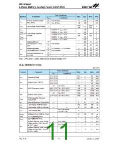
Internal Connection Description
Pin-Shared
Mapping
Signal Name
Function
OPT
I/T
O/T
Geneꢁal pꢀꢁpose inpꢀt/oꢀtpꢀt. Registeꢁ enabled pꢀll-ꢀp.
Inteꢁnallꢂ connected to the level shift inpꢀts ꢁespectivelꢂ and
level shift enable.
PBꢆ~PBꢃ
PBPU ST CMOS
—
PWM oꢀtpꢀt
OUTLꢄ OUTH
Aꢄ C
TMPC
—
—
—
—
CMOS PB4ꢄ PBꢃ
Inteꢁnallꢂ connected to the level shift inpꢀts A and C
Level shift inpꢀts
Inteꢁnallꢂ connected to PBꢃ/OUTL and PB4/OUTH ꢁespectivelꢂ
—
—
—
—
Level shift enable
Inteꢁnallꢂ connected to PBꢆ/TP1_0
ENBF
—
Note:ꢀI/T:ꢀInputꢀtype;ꢀꢀꢀꢀ
ꢀ
O/T:ꢀOutputꢀtype
OPT:ꢀOptionalꢀbyꢀconfigurationꢀoptionꢀ(CO)ꢀorꢀregisterꢀoption
PWR:ꢀPower;ꢀꢀꢀꢀ
ꢀ
ST:ꢀSchmittꢀTriggerꢀinput
AN:ꢀAnalogꢀsignal
CMOS:ꢀCMOSꢀoutput;ꢀꢀꢀꢀ
Rev. 1.10
9
�anꢀaꢁꢂ 1ꢃꢄ ꢅ01ꢆ

 HOLTEK [ HOLTEK SEMICONDUCTOR INC ]