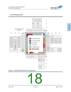
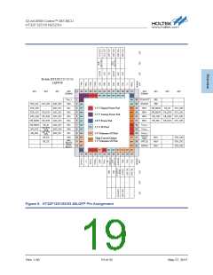
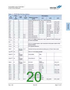
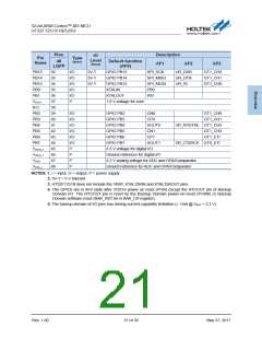
32-bit ARM Cortex™-M3 MCU
HT32F1251/51B/52/53
Electrical Characteristics
4
Absolute Maximum Ratings
The following table shows the absolute maximum ratings of the device. These are stress ratings
only. Stresses beyond absolute maximum ratings may cause permanent damage to the device. Note
that the device is not guaranteed to operate properly at the maximum ratings. Exposure to the
absolute maximum rating conditions for extended periods may affect device reliability.
Table 3. Absolute Maximum Ratings
Symbol
VDD33
Parameter
Min
VSS - 0.3
VSSA - 0.3
VSS - 0.3
VSS - 0.3
VSS - 0.3
-40
Max
VSS + 3.6
VSSA + 3.6
VSS + 3.6
VSS + 5.5
VDD33 + 0.3
+85
Unit
V
External main supply voltage
VDDA
External analog supply voltage
External battery supply voltage
Input voltage on 5 V-tolerant I/O
Input voltage on other I/O
V
VBAT
V
V
VIN
V
TA
Operating temperature range
Storage temperature range
°C
°C
°C
mW
V
TSTG
TJ
-55
+150
Maximum junction temperature
Total power dissipation
—
125
PD
—
500
VESD
Electrostatic discharge voltage (human body mode)
-4000
+4000
DC Characteristics
Table 4. DC Operating Conditions
TA = 25°C, unless otherwise specified.
Symbol
VDD33
Parameter
Operating voltage of I/O
Analog operating voltage
Conditions
Min
2.7
Typ
3.3
3.3
3.3
1.8
Max
3.6
Unit
V
—
—
VDDA
2.7
3.6
V
VBAT
Operating voltage of Battery supply —
Operating voltage of core power
2.7
3.6
V
VDD18
—
1.62
1.98
V
On-Chip LDO Voltage Regulator Characteristics
Table 5. LDO Characteristics
TA = 25°C, unless otherwise specified.
Symbol
VLDOOUT
IDD18
Parameter
Conditions
Min
1.71
—
Typ
1.8
—
Max
1.89
200
Unit
V
Internal regulator output
voltage
VLDOIN = 3.3 V Regulator input
Output current
VLDOIN = 2.4 V Regulator input
mA
External filter capacitor
value for internal core
power supply
The capacitor value is
dependent on the core power
current consumption
CLDO
2.2
—
10
μF
Rev. 1.00
22 of 35
May 27, 2011

 HOLTEK [ HOLTEK SEMICONDUCTOR INC ]