32-bit ARM Cortex™-M3 MCU
HT32F1251/51B/52/53
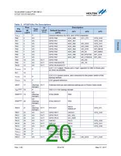
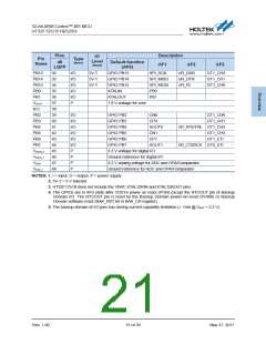
Pins
Description
AF1
IO
Pin
Name
Type
Level
48
LQFP
Default function
(AF0)
(Note1)
AF2
AF3
(Note2)
PB13
PB14
PB15
PB0
32
I/O
5V-T
GPIO PB13
GPIO PB14
GPIO PB15
XTALIN
SPI_SCK
SPI_MISO
SPI_MOSI
PB0
UR_DSR
UR_DTR
UR_RI
GT1_CH2
GT1_CH1
GT1_CH0
33
34
35
36
37
38
39
40
41
42
43
44
45
46
47
48
I/O
I/O
I/O
I/O
P
5V-T
5V-T
PB1
XTALOUT
PB1
VDD18
N.C
1.8 V voltage for core
PB2
I/O
I/O
I/O
I/O
I/O
I/O
P
GPIO PB2
GPIO PB3
GPIO PB4
GPIO PB5
GPIO PB6
GPIO PB7
CN0
GT1_CH0
GT1_CH1
PB3
CP0
PB4
AOUT0
CN1
UR_RTS/TXE GT1_CH2
GT1_CH3
PB5
PB6
CP1
GT1_ETI
PB7
AOUT1
UR_CTS/SCK GT0_ETI
VDD33_1
VSS33_1
VDDA
3.3 V voltage for digital I/O
P
Ground reference for digital I/O
P
3.3 V analog voltage for ADC and OPA/Comparator
Ground reference for ADC and OPA/Comparator
VSSA_1
P
NOTES: 1. I = input, O = output, P = power supply.
2. 5V-T = 5 V tolerant.
3. HT32F1251B does not include the VBAT, XTAL32KIN and XTAL32KOUT pins.
4. The GPIOs are in AF0 state after VDD18 power on reset (POR) except the RTCOUT pin of Backup
Domain I/O. The RTCOUT pin is reset by the Backup Domain power-on-reset (PORB) or Backup
Domain software reset (BAK_RST bit in BAK_CR register).
5. The backup domain of I/O pins has driving current capability limitation (< 1mA @ VBAT = 3.3 V).
Rev. 1.00
21 of 35
May 27, 2011

 HOLTEK [ HOLTEK SEMICONDUCTOR INC ]