HT1380A/HT1381A
dataꢀcanꢀbeꢀwrittenꢀtoꢀtheꢀregisterꢀarray.ꢀTheseꢀtwoꢀ
bitsꢀshouldꢀfirstꢀbeꢀspecifiedꢀinꢀorderꢀtoꢀreadꢀfromꢀandꢀ
writeꢀtoꢀtheꢀregisterꢀarrayꢀproperly.
Functional Description
Theꢀ HT1380A/HT1381Aꢀ mainlyꢀ containsꢀ theꢀ
followingꢀinternalꢀelements:ꢀaꢀdataꢀshiftꢀregisterꢀarrayꢀ
toꢀstoreꢀtheꢀclock/calendarꢀdata,ꢀcommandꢀcontrolꢀ
logic,ꢀoscillatorꢀcircuitꢀandꢀreadꢀtimerꢀclock.ꢀTheꢀ
clockꢀisꢀcontainedꢀinꢀeightꢀread/writeꢀregistersꢀasꢀ
shownꢀbelow.ꢀDataꢀcontainedꢀinꢀtheꢀclockꢀregisterꢀisꢀ
inꢀbinaryꢀcodedꢀdecimalꢀformat.
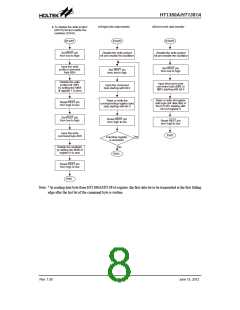
Command Byte
Forꢀeachꢀdataꢀtransfer,ꢀaꢀCommandꢀByteꢀisꢀinitiatedꢀ
toꢀspecifyꢀwhichꢀregisterꢀisꢀaccessed.ꢀThisꢀisꢀtoꢀ
determineꢀwhetherꢀaꢀread,ꢀwrite,ꢀorꢀtestꢀcycleꢀisꢀ
operatedꢀandꢀwhetherꢀaꢀsingleꢀbyteꢀorꢀburstꢀmodeꢀ
transferꢀisꢀtoꢀoccur.ꢀReferꢀtoꢀtheꢀtableꢀshownꢀbelowꢀ
andꢀfollowꢀtheꢀstepsꢀtoꢀwriteꢀtheꢀdataꢀtoꢀtheꢀchip.ꢀFirstꢀ
giveꢀaꢀCommandꢀByteꢀofꢀHT1380A/HT1381A,ꢀandꢀ
thenꢀwriteꢀaꢀdataꢀinꢀtheꢀregister.
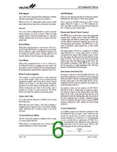
Twoꢀmodesꢀareꢀavailableꢀforꢀtransferringꢀtheꢀdataꢀ
betweenꢀtheꢀmicroprocessorꢀandꢀtheꢀHT1380A/
HT1381A.ꢀOneꢀisꢀinꢀsingle-byteꢀmodeꢀandꢀtheꢀotherꢀisꢀ
inꢀmultiple-byteꢀmode.
Thisꢀ tableꢀ illustratesꢀ theꢀ correlationꢀ betweenꢀ
CommandꢀByteꢀandꢀtheirꢀbits:
TheꢀHT1380A/HT1381Aꢀalsoꢀcontainsꢀtwoꢀadditionalꢀ
bits,ꢀtheꢀclockꢀhaltꢀbitꢀ(CH)ꢀandꢀtheꢀwriteꢀprotectꢀbitꢀ(WP).ꢀ
Theseꢀbitsꢀcontrolꢀtheꢀoperationꢀofꢀtheꢀoscillatorꢀandꢀsoꢀ
Command Byte
Function Description
C7
—
—
C
C6
—
—
—
0
C5
—
—
—
0
C4
—
—
—
1
C3
—
A2
—
x
C2
—
A1
—
x
C1
—
A0
—
x
C0
R/W
—
Select Read or Write Cycle
Specify the Register to be Accessed
Clock Halt Flag
—
For IC Test Only
1
1
Select Single Byte or Burst Mode
1
0
1
1
1
1
1
x
Note:ꢀ″x″ꢀstandsꢀforꢀdon′tꢀcare
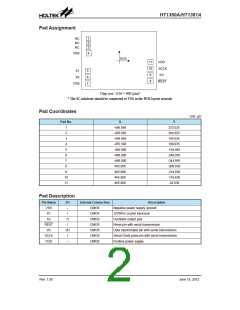
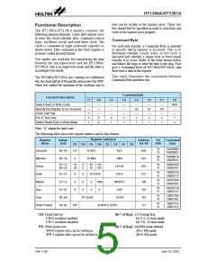
Theꢀfollowingꢀtableꢀshowsꢀtheꢀregisterꢀaddressꢀandꢀitsꢀdataꢀformat:
Register Definition
Register
Name
Range
Data
Address
A2~A0
Bit
R/W
Command
Byte
D7
D6
D5
D4
D3
D2
D1
D0
W
R
10000000
10000001
Seconds
00~59
00~59
CH
10 SEC
SEC
000
W
R
10000010
10000011
Minutes
Hours
0
10 MIN
MIN
HOUR
DATE
MONTH
DAY
001
010
011
100
101
110
111
01~12
00~23
12\
24
0
0
AP HR
10 HR
W
R
10000100
10000101
W
R
10000110
10000111
Date
01~31
01~12
01~07
00~99
00~80
0
0
0
0
0
0
10 DATE
W
R
10001000
10001001
Month
Day
0
0
10M
0
W
R
10001010
10001011
W
R
10001100
10001101
Year
10 YEAR
YEAR
W
R
10001110
10001111
Write Protect
WP
ALWAYS ZERO
CH:ꢀClockꢀHaltꢀbit
Bit 7 of Reg2:ꢀ12/24ꢀmodeꢀflag
ꢀꢀꢀꢀꢀꢀꢀꢀꢀꢀꢀꢀꢀꢀCH=0ꢀoscillatorꢀenabled
ꢀꢀꢀꢀꢀꢀꢀꢀꢀꢀꢀꢀꢀꢀCH=1ꢀoscillatorꢀdisabled
ꢀ
ꢀ
ꢀꢀꢀꢀꢀꢀꢀꢀꢀꢀꢀꢀꢀꢀbitꢀ7=1,ꢀ12-hourꢀmode
ꢀꢀꢀꢀꢀꢀꢀꢀꢀꢀꢀꢀꢀꢀbitꢀ7=0,ꢀ24-hourꢀmode
WP:ꢀWriteꢀprotectꢀbit
ꢀꢀꢀꢀꢀꢀꢀꢀꢀꢀꢀꢀꢀꢀWP=0ꢀregisterꢀdataꢀcanꢀbeꢀwrittenꢀinꢀ
ꢀꢀꢀꢀꢀꢀꢀꢀꢀꢀꢀꢀꢀꢀWP=1ꢀregisterꢀdataꢀcanꢀnotꢀbeꢀwrittenꢀin
Bit 5 of Reg2:ꢀAM/PMꢀmodeꢀdefined
ꢀꢀꢀꢀꢀꢀꢀꢀꢀꢀꢀꢀꢀꢀAP=1ꢀPMꢀmode
ꢀ
ꢀ
ꢀꢀꢀꢀꢀꢀꢀꢀꢀꢀꢀꢀꢀꢀAP=0ꢀAMꢀmode
Rev. 1.00
5
June 15, 2012

 HOLTEK [ HOLTEK SEMICONDUCTOR INC ]