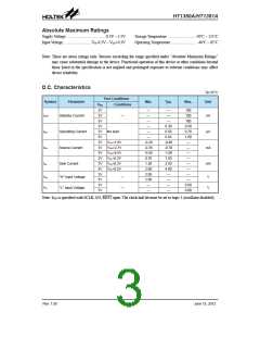
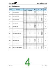
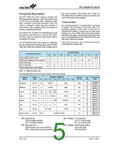
HT1380A/HT1381A
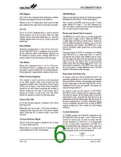
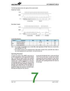
Theꢀfollowingꢀdiagramꢀshowsꢀtheꢀsingleꢀandꢀburstꢀmodeꢀtransfer:
Single Byte Transfer
S
L
C
K
R
S
E
T
0
1
2
3
5
4
6
0
7
1
2
3
4
6
5
7
I
O
/
0
R
W
/
A
0
A
1
A
2
0
0
1
C
m
o
m
a
n
B
y
d
t
e
D
t
a
a
I
/
O
Burst Mode Transfer
S
L
C
K
R
S
E
T
0
1
2
3
5
4
6
0
7
7
0
7
I
O
/
R
W
/
1
1
1
1
1
0
1
C
m
o
m
a
n
B
d
t
y
e
D
t
a
a
B
y
e
t
0
D
t
a
a
B
y
e
t
7
Crystal Specifications
Symbol
Parameter
Min.
—
Typ.
Max.
—
Unit
kHz
kΩ
fO
Nominal Frequency
Series Resistance
Load Capacitance
32.768
—
ESR
CL
—
50
—
9.0
—
pF
Note:ꢀ1.ꢀItꢀisꢀstronglyꢀrecommendedꢀtoꢀuseꢀaꢀcrystalꢀwithꢀaꢀloadꢀcapacitanceꢀofꢀ9.0pF.ꢀNeverꢀuseꢀaꢀcrystalꢀwithꢀaꢀ
loadꢀcapacitanceꢀofꢀ12.5pF.
2.ꢀTheꢀoscillatorꢀselectionꢀcanꢀbeꢀoptimizedꢀusingꢀaꢀhighꢀqualityꢀresonatorꢀwithꢀaꢀsmallꢀESRꢀvalue.ꢀReferꢀtoꢀ
theꢀcrystalꢀmanufacturerꢀforꢀmoreꢀdetails:ꢀwww.microcrystal.com.
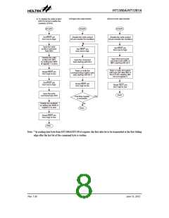
Operating Flowchart
InꢀusingꢀtheꢀHT1380A/HT1381A,ꢀsetꢀfirstꢀtheꢀWPꢀandꢀ
CHꢀtoꢀ0ꢀandꢀwaitꢀforꢀaboutꢀ3ꢀseconds,ꢀtheꢀoscillatorꢀ
willꢀgenerateꢀtheꢀclocksꢀforꢀinternalꢀuse.ꢀThen,ꢀchooseꢀ
eitherꢀsingleꢀmodeꢀorꢀburstꢀmodeꢀtoꢀinputꢀtheꢀdata.ꢀ
Theꢀreadꢀorꢀwriteꢀoperatingꢀflowchartsꢀareꢀshownꢀonꢀ
theꢀnextꢀpage.
Toꢀinitiateꢀanyꢀtransferꢀofꢀdata,ꢀRESTꢀisꢀtakenꢀhighꢀandꢀ
anꢀ8-bitꢀcommandꢀbyteꢀisꢀfirstꢀloadedꢀintoꢀtheꢀcontrolꢀ
logicꢀtoꢀprovideꢀtheꢀregisterꢀaddressꢀandꢀcommandꢀ
information.ꢀFollowingꢀtheꢀcommandꢀword,ꢀtheꢀclock/
calendarꢀdataꢀisꢀseriallyꢀtransferredꢀtoꢀorꢀfromꢀtheꢀ
correspondingꢀregister.ꢀTheꢀRESTꢀpinꢀmustꢀbeꢀtakenꢀ
lowꢀagainꢀafterꢀtheꢀtransferꢀoperationꢀisꢀcompleted.ꢀAllꢀ
dataꢀenterꢀonꢀtheꢀrisingꢀedgeꢀofꢀSCLKꢀandꢀoutputsꢀonꢀ
theꢀfallingꢀedgeꢀofꢀSCLK.ꢀInꢀtotal,ꢀ16ꢀclockꢀpulsesꢀareꢀ
neededꢀforꢀaꢀsingleꢀbyteꢀmodeꢀandꢀ72ꢀforꢀburstꢀmode.ꢀ
Bothꢀinputꢀandꢀoutputꢀdataꢀstartsꢀwithꢀbitꢀ0.
Rev. 1.00
7
June 15, 2012

 HOLTEK [ HOLTEK SEMICONDUCTOR INC ]