HT1380A/HT1381A
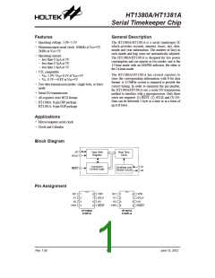
Pad Assignment
N
N
N
C
C
C
1
2
3
V
S
S
4
(
,
0
)
0
1
1
V
D
D
1
0
S
L
C
K
X
1
5
9
I
/
O
X
2
6
8
R
E
S
T
V
S
S
7
Chipꢀsize:ꢀ1136ꢀ×ꢀ900ꢀ(μm)2
*ꢀTheꢀICꢀsubstrateꢀshouldꢀbeꢀconnectedꢀtoꢀVSSꢀinꢀtheꢀPCBꢀlayoutꢀartwork.
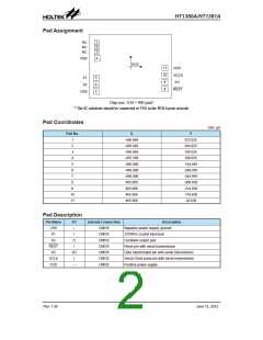
Pad Coordinates
Unit: μm
Pad No.
X
Y
1
2
-456.985
-456.985
-456.985
-455.590
-466.000
-466.000
-466.000
465.966
465.966
465.966
465.966
333.025
264.025
195.025
109.935
-154.955
-249.955
-344.955
-309.630
-214.630
-119.630
-24.630
3
4
5
6
7
8
9
10
11
Pad Description
Pin Name
I/O
�
I
Internal Connection
CMOS
Description
VSS
Negative power supply, ground
32768Hz crystal input pad
Oscillator output pad
X1
CMOS
X2
O
I
CMOS
REST
I/O
CMOS
Reset pin with serial transmission
I/O
I
CMOS
Data Input/Output pin with serial transmission
Serial Clock pulse pin with serial transmission
Positive power supply
SCLK
VDD
CMOS
�
CMOS
Rev. 1.00
2
June 15, 2012

 HOLTEK [ HOLTEK SEMICONDUCTOR INC ]