15.5
Interrupts
The A/D converter generates an interrupt (ADI) at the end of A/D conversion. The ADI interrupt
request can be enabled or disabled by the ADIE bit in ADCSR.
15.6
Application Notes
When using the A/D converter, note the following points.
Setting Ranges of Analog Power Supply and Other Pins:
1. Analog Input Voltage Range
During A/D conversion, the voltages input to the analog input pins ANn should be in the range
AVSS ≤ ANn ≤ AVref. (n = 0 to 7)
2. AVCC and AVSS Input Voltages
AVSS should be equal to VSS. If the A/D converter is not used, the values should be AVCC = VCC
and AVSS = VSS
3. AVref Input Range
The analog reference voltage input at the AVref pin should be in the range AVref ≤ AVCC. If the
A/D converter is not used, the value should be AVref = VCC.
Notes on Board Design: In board design, digital circuitry and analog circuitry should be as
mutually isolated as possible, and layout in which digital circuit signal lines and analog circuit
signal lines cross or are in close proximity should be avoided as far as possible. Failure to do so
may result in incorrect operation of the analog circuitry due to inductance, adversely affecting A/D
conversion values.
Also, digital circuitry must be isolated from the analog input signals (AN0 to AN7), analog
reference voltage (AVref), and analog power supply (AVCC) by the analog ground (AVSS). The
analog ground (AVSS) should be connected to a stable digital ground (VSS) at one point on the
board.
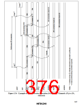
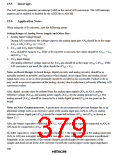
Notes on Noise Countermeasures: A protection circuit connected to prevent damage due to an
abnormal voltage such as an excessive surge at the analog input pins (AN0 to AN7) or analog
reference power supply pin (AVref) should be connected between AVCC and AVSS as shown in
figure 15.7.
Also, the bypass capacitors connected to AVCC, AVref and the filter capacitor connected to AN0 to
AN7 must be connected to AVSS.
If a filter capacitor is connected as shown in figure 15.7, the input currents at the analog input pins
(AN0 to AN7) are averaged, and so an error may arise. Also, when A/D conversion is performed
frequently, as in scan mode, if the current charged and discharged by the capacitance of the
sample-and-hold circuit in the A/D converter exceeds the current input via the input impedance
350

 HITACHI [ HITACHI SEMICONDUCTOR ]