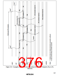
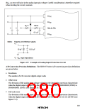
(Rin), an error will arise in the analog input pin voltage. Careful consideration is therefore required
when deciding the circuit constants.
AVCC
AVref
Rin*2
100 Ω
0.1 µF
1
1
AN0 to AN7
AVSS
*
*
Notes: Figures are reference values.
*1
10 µF
0.01 µF
*2 Rin: Input impedance
Figure 15.7 Example of Analog Input Protection Circuit
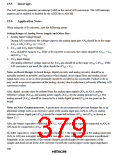
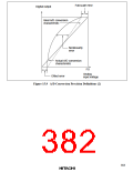
A/D Conversion Precision Definitions: The H8/3437 Series A/D conversion precision definitions
are given below.
•
•
Resolution
The number of A/D converter digital output codes
Offset error
The deviation of the analog input voltage value from the ideal A/D conversion characteristic
when the digital output changes from the minimum voltage value B'0000000000 (H'000) to
B'0000000001 (H'001) (see figure 15.9).
•
Full-scale error
The deviation of the analog input voltage value from the ideal A/D conversion characteristic
when the digital output changes from B'1111111110 (H'3FE) to B'1111111111 (H'3FF) (see
figure 15.9).
351

 HITACHI [ HITACHI SEMICONDUCTOR ]