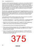
Table 15.4 A/D Conversion Time (Single Mode)
CKS
=
0CKS
Symbol
tD
Min
10
Typ
—
Max
17
Min
6
Typ
—
Max
9
Synchronization delay
Input sampling time*
A/D conversion time*
tSPL
—
80
—
—
—
40
—
—
tCONV
259
266
131
134
Note: Values in the table are numbers of states.
* Values for when øP = ø. When øP = ø/2, values are double those given in the table.
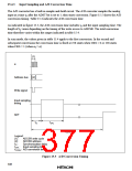
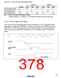
15.4.4 External Trigger Input Timing
A/D conversion can be externally triggered. When the TRGE bit is set to 1 in ADCR, external
trigger input is enabled at the ADTRG pin. A high-to-low transition at the ADTRG pin sets the
ADST bit to 1 in ADCSR, starting A/D conversion. Other operations, in both single and scan
modes, are the same as if the ADST bit had been set to 1 by software. Figure 15.6 shows the
timing.
ø
ADTRG
Internal trigger
signal
ADST
A/D conversion
Figure 15.6 External Trigger Input Timing
349

 HITACHI [ HITACHI SEMICONDUCTOR ]