15.4.2 Scan Mode (SCAN = 1)
Scan mode is useful for monitoring analog inputs in a group of one or more channels. When the
ADST bit is set to 1 by software or external trigger input, A/D conversion starts on the first
channel in the group (AN0 when CH2 = 0, AN4 when CH2 = 1). When two or more channels are
selected, after conversion of the first channel ends, conversion of the second channel (AN1 or
AN5) starts immediately. A/D conversion continues cyclically on the selected channels until the
ADST bit is cleared to 0. The conversion results are transferred for storage into the A/D data
registers corresponding to the channels.
When the mode or analog input channel selection must be changed during analog conversion, to
prevent incorrect operation, first clear the ADST bit to 0 in ADCSR to halt A/D conversion. After
making the necessary changes, set the ADST bit to 1. A/D conversion will start again from the
first channel in the group. The ADST bit can be set at the same time as the mode or channel
selection is changed.
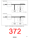
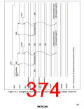
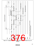
Typical operations when three channels in group 0 (AN0 to AN2) are selected in scan mode are
described next. Figure 15.4 shows a timing diagram for this example.
1. Scan mode is selected (SCAN = 1), scan group 0 is selected (CH2 = 0), analog input channels
AN0 to AN2 are selected (CH1 = 1, CH0 = 0), and A/D conversion is started (ADST = 1).
2. When A/D conversion of the first channel (AN0) is completed, the result is transferred into
ADDRA. Next, conversion of the second channel (AN1) starts automatically.
3. Conversion proceeds in the same way through the third channel (AN2).
4. When conversion of all selected channels (AN0 to AN2) is completed, the ADF flag is set to 1
and conversion of the first channel (AN0) starts again. If the ADIE bit is set to 1, an ADI
interrupt is requested at this time.
5. Steps 2 to 4 are repeated as long as the ADST bit remains set to 1. When the ADST bit is
cleared to 0, A/D conversion stops. After that, if the ADST bit is set to 1, A/D conversion
starts again from the first channel (AN0).
346

 HITACHI [ HITACHI SEMICONDUCTOR ]