14.3
Operation
14.3.1 Host Interface Operation
The host interface is activated by setting the HIE bit (bit 1) to 1 in SYSCR, establishing slave
mode. Activation of the host interface (entry to slave mode) appropriates the related I/O lines in
port 3 or B (data), port 8 or 9 (control) and port 4 (host interrupt requests) for interface use.
For host interface read/write timing diagrams, see section 23.3.8, Host Interface Timing.
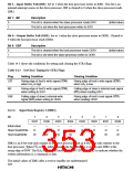
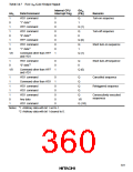
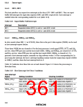
14.3.2 Control States
Table 14.5 indicates the slave operations carried out in response to host interface signals from the
host processor.
Table 14.5 Host Interface Operation
CS2
CS1
IOR
IOW
HA0
0
Slave Operation
1
0
0
0
Prohibited
1
Prohibited
1
0
1
0
1
0
1
0
Data read from output data register 1 (ODR1)
Status read from status register 1 (STR1)
Data write to input data register 1 (IDR1)
Command write to input data register 1 (IDR1)
Idle state
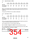
1
1
0
1
0
1
0
1
Idle state
0
1
0
Prohibited
1
Prohibited
0
Data read from output data register 2 (ODR2)
Status read from status register 2 (STR2)
Data write to input data register 2 (IDR2)
Command write to input data register 2 (IDR2)
Idle state
1
0
1
0
1
Idle state
328

 HITACHI [ HITACHI SEMICONDUCTOR ]