8.4.5
Timing of Input Capture Flag (ICF) Setting
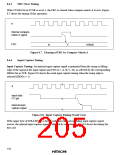
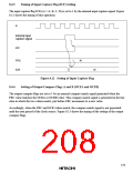
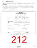
The input capture flag ICFx (x = A, B, C, D) is set to 1 by the internal input capture signal. Figure
8.12 shows the timing of this operation.
ø
Internal input
capture signal
ICF
FRC
ICR
N
N
Figure 8.12 Setting of Input Capture Flag
8.4.6
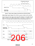
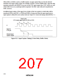
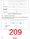
Setting of Output Compare Flags A and B (OCFA and OCFB)
The output compare flags are set to 1 by an internal compare-match signal generated when the
FRC value matches the OCRA or OCRB value. This compare-match signal is generated at the last
state in which the two values match, just before FRC increments to a new value.
Accordingly, when the FRC and OCR values match, the compare-match signal is not generated
until the next period of the clock source. Figure 8.13 shows the timing of the setting of the output
compare flags.
179

 HITACHI [ HITACHI SEMICONDUCTOR ]