When ICRC or ICRD is used as a buffer register, its input capture flag is set by the selected
transition of its input capture signal. For example, if ICRC is used to buffer ICRA, when the edge
transition selected by the IEDGC bit occurs on the FTIC input capture line, ICFC will be set, and
if the ICIEC bit is set, an interrupt will be requested. The FRC value will not be transferred to
ICRC, however.
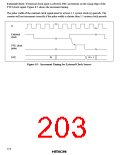
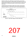
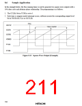
In buffered input capture, if the upper byte of either of the two registers to which data will be
transferred (ICRA and ICRC, or ICRB and ICRD) is being read when the input signal arrives,
input capture is delayed by one system clock (ø). Figure 8.11 shows the timing when BUFEA = 1.
Read cycle:
CPU reads upper byte of ICRA or ICRC
T1
T2
T3
ø
Input at
FTIA pin
Internal input
capture signal
Figure 8.11 Input Capture Timing (1-State Delay, Buffer Mode)
178

 HITACHI [ HITACHI SEMICONDUCTOR ]