8.4.3
FRC Clear Timing
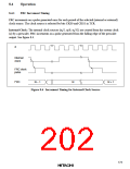
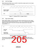
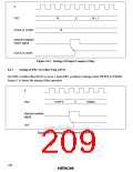
If the CCLRA bit in TCSR is set to 1, the FRC is cleared when compare-match A occurs. Figure
8.7 shows the timing of this operation.
ø
Internal compare-
match A signal
FRC
N
H'0000
Figure 8.7 Clearing of FRC by Compare-Match A
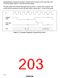
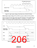
Input Capture Timing
8.4.4
Input Capture Timing: An internal input capture signal is generated from the rising or falling
edge of the signal at the input capture pin FTIx (x = A, B, C, D), as selected by the corresponding
IEDGx bit in TCR. Figure 8.8 shows the usual input capture timing when the rising edge is
selected (IEDGx = 1).
ø
Input data
FTI pin
Internal input
capture signal
Figure 8.8 Input Capture Timing (Usual Case)
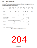
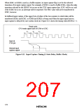
If the upper byte of ICRA/B/C/D is being read when the corresponding input capture signal
arrives, the internal input capture signal is delayed by one state. Figure 8.9 shows the timing for
this case.
176

 HITACHI [ HITACHI SEMICONDUCTOR ]