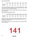
7.4
Port 3
7.4.1
Overview
Port 3 is an 8-bit input/output port that is multiplexed with the data bus and host interface data bus.
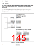
Figure 7.9 shows the pin configuration of port 3. The pin functions differ depending on the
operating mode.
Port 3 has built-in, programmable MOS input pull-up transistors that can be used in mode 3.
Pins in port 3 can drive one TTL load and a 90-pF capacitive load. They can also drive a
darlington transistor.
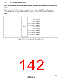
Pin configuration in mode 1
(expanded mode with on-chip
ROM disabled) and mode 2
(expanded mode with on-chip
Port 3 pins
ROM enabled)
P37/D7/HDB7
P36/D6/HDB6
P35/D5/HDB5
P34/D4/HDB4
P33/D3/HDB3
P32/D2/HDB2
P31/D1/HDB1
P30/D0/HDB0
D7 (input/output)
D6 (input/output)
D5 (input/output)
D4 (input/output)
D3 (input/output)
D2 (input/output)
D1 (input/output)
D0 (input/output)
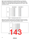
Port 3
Pin configuration in mode 3 (single-chip mode)
Master mode
Slave mode
P37 (input/output)
P36 (input/output)
P35 (input/output)
P34 (input/output)
P33 (input/output)
P32 (input/output)
P31 (input/output)
P30 (input/output)
HDB7 (input/output)
HDB6 (input/output)
HDB5 (input/output)
HDB4 (input/output)
HDB3 (input/output)
HDB2 (input/output)
HDB1 (input/output)
HDB0 (input/output)
Figure 7.9 Port 3 Pin Configuration
116

 HITACHI [ HITACHI SEMICONDUCTOR ]