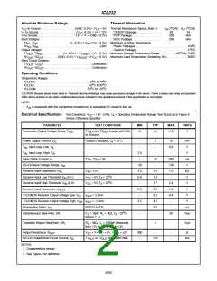
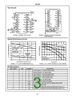
ICL232
Pin Descriptions (Continued)
PDIP, CERDIP
SOIC
PIN NAME
DESCRIPTION
12
13
14
15
16
12
R1
Receiver 1 TTL/CMOS output.
OUT
13
R1
RS-232 Receiver 1 input, with internal 5K pulldown resistor to GND.
RS-232 Transmitter 1 output ±10V (typical).
Supply Ground.
IN
14
T1
OUT
15
GND
16
V
Positive Power Supply +5V ±10%
CC
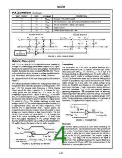
VOLTAGE DOUBLER
+
VOLTAGE INVERTER
+
S5
S1
S3
S2
C2
C1
V+ = 2V
S6
CC
V
GND
CC
+
+
+
+
C3
C2
C4
C1
-
-
-
-
V
GND
CC
V- = -(V+)
GND
C1-
S4
C2-
S7
S8
RC
OSCILLATOR
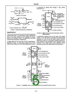
FIGURE 5. DUAL CHARGE PUMP
Detailed Description
The ICL232 is a dual RS-232 transmitter/receiver powered by Transmitters
a single +5V power supply which meets all ElA RS232C spec-
The transmitters are TTL/CMOS compatible inverters which
translate the inputs to RS-232 outputs. The input logic thresh-
ifications and features low power consumption. The functional
diagram illustrates the major elements of the ICL232. The cir-
cuit is divided into three sections: a voltage doubler/inverter,
dual transmitters, and dual receivers Voltage Converter.
old is about 26% of V , or 1.3V for V
= 5V. A logic 1 at
CC CC
the input results in a voltage of between -5V and V- at the out-
put, and a logic 0 results in a voltage between +5V and (V+
An equivalent circuit of the dual charge pump is illustrated in - 0.6V). Each transmitter input has an internal 400kΩ pullup
Figure 5.
resistor so any unused input can be left unconnected and its
output remains in its low state. The output voltage swing
meets the RS-232C specification of ±5V minimum with the
worst case conditions of: both transmitters driving 3kΩ mini-
The voltage quadrupler contains two charge pumps which use
two phases of an internally generated clock to generate +10V
and -10V. The nominal clock frequency is 16kHz. During
phase one of the clock, capacitor C1 is charged to V
During phase two, the voltage on C1 is added to V
producing a signal across C2 equal to twice V . At the same
time, C3 is also charged to 2V , and then during phase one,
CC
mum load impedance, V
= 4.5V, and maximum allowable
CC
.
,
CC
CC
operating temperature. The transmitters have an internally
limited output slew rate which is less than 30V/µs. The outputs
are short circuit protected and can be shorted to ground indef-
initely. The powered down output impedance is a minimum of
CC
it is inverted with respect to ground to produce a signal across
C4 equal to -2V . The voltage converter accepts input
300Ω with ±2V applied to the outputs and V
= 0V.
CC
CC
voltages up to 5.5V. The output impedance of the doubler (V+)
is approximately 200Ω, and the output impedance of the
inverter (V-) is approximately 450Ω. Typical graphs are
presented which show the voltage converters output vs input
voltage and output voltages vs load characteristics. The test
circuit (Figure 3) uses 1µF capacitors for C1-C4, however, the
value is not critical. Increasing the values of C1 and C2 will
lower the output impedance of the voltage doubler and
inverter, and increasing the values of the reservoir capacitors,
C3 and C4, lowers the ripple on the V+ and V- supplies.
V+
V
CC
400kΩ
300Ω
T
XIN
T
OUT
GND < T
< V
CC
XIN
V-
V- < V
< V+
TOUT
FIGURE 7. TRANSMITTER
Receivers
The receiver inputs accept up to ±30V while presenting the
required 3kΩ to 7kΩ input impedance even it the power is off
T1 , T2
IN
IN
(V
= 0V). The receivers have a typical input threshold of
CC
90%
10%
V
OH
T1
, T2
1.3V which is within the ±3V limits, known as the transition
region, of the RS-232 specification. The receiver output is
0V to V . The output will be low whenever the input is
greater than 2.4V and high whenever the input is floating or
driven between +0.8V and -30V. The receivers feature 0.5V
hysteresis to improve noise rejection.
OUT
OUT
V
OL
t
t
f
r
CC
(0.8) (V
OH
- V
OL
)
(0.8) (V - V )
OL OH
Instantaneous
Slew Rate (SR)
=
or
t
t
f
r
FIGURE 6. SLEW RATE DEFINITION
8-52

 HARRIS [ HARRIS CORPORATION ]