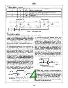
ICL232
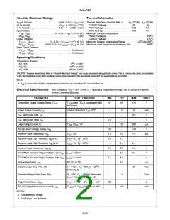
Absolute Maximum Ratings
Thermal Information
o
o
V
to Ground . . . . . . . . . . . . . . . . . . . . . .(GND -0.3V) < V
< 6V Thermal Resistance (Typical, Note 1)
θ
( C/W)
θ
( C/W)
CC
V+ to Ground . . . . . . . . . . . . . . . . . . . . . . . (V
CC
-0.3V) < V+ < 12V
JA
JC
CERDIP Package . . . . . . . . . . . . . . . .
PDIP Package . . . . . . . . . . . . . . . . . . .
SOIC Package. . . . . . . . . . . . . . . . . . .
Maximum Junction Temperature
80
100
100
18
N/A
N/A
CC
V- to Ground . . . . . . . . . . . . . . . . . . . . . . . -12V < V- < (GND +0.3V)
Input Voltages
T1 , T2 . . . . . . . . . . . . . . . . . . . . (V- -0.3V) < V < (V+ +0.3V)
IN IN IN
o
R1 , R2 . . . . . . . . . . . . . . . . . . . . . . . . . . . . . . . . . . . . . . ±30V
Plastic Packages . . . . . . . . . . . . . . . . . . . . . . . . . . . . . . . . . 150 C
Ceramic Package . . . . . . . . . . . . . . . . . . . . . . . . . . . . . . . . 175 C
Maximum Storage Temperature Range . . . . . . . . . .-65 C to 150 C
Maximum Lead Temperature (Soldering 10s) . . . . . . . . . . . . . 300 C
IN IN
o
Output Voltages
T1 , T2
o
o
. . . . . . . . . . . . (V- -0.3V) < V
< (V+ +0.3V)
< (V +0.3V)
OUT OUT
TXOUT
o
R1
, R2
. . . . . . . . .(GND -0.3V) < V
OUT OUT
RXOUT
CC
Short Circuit Duration
T1 , T2
. . . . . . . . . . . . . . . . . . . . . . . . . . . . . . Continuous
. . . . . . . . . . . . . . . . . . . . . . . . . . . . . . Continuous
OUT
OUT
R1
OUT
, R2
OUT
Operating Conditions
Temperature Ranges
ICL232C . . . . . . . . . . . . . . . . . . . . . . . . . . . . . . . . . . .0 C to 70 C
ICL232I . . . . . . . . . . . . . . . . . . . . . . . . . . . . . . . . . . -40 C to 85 C
ICL232M . . . . . . . . . . . . . . . . . . . . . . . . . . . . . . . . -55 C to 125 C
o
o
o
o
o
o
CAUTION: Stresses above those listed in “Absolute Maximum Ratings” may cause permanent damage to the device. This is a stress only rating and operation
of the device at these or any other conditions above those indicated in the operational sections of this specification is not implied.
NOTE:
1. θ is measured with the component mounted on an evaluation PC board in free air.
JA
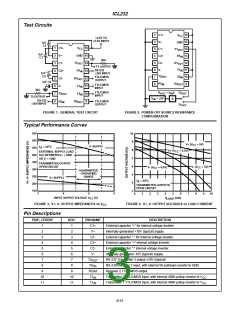
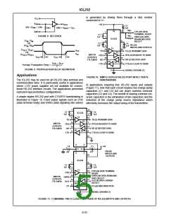
Electrical Specifications Test Conditions: V = +5V ±10%, T = Operating Temperature Range. Test Circuit as in Figure 8
CC
A
Unless Otherwise Specified
PARAMETER
TEST CONDITIONS
MIN
TYP
MAX
UNITS
Transmitter Output Voltage Swing, T
T1
and T2
OUT
Loaded with 3kΩ
±5
±9
±10
V
OUT
OUT
to Ground
o
Power Supply Current, I
Outputs Unloaded, T = 25 C
-
-
5
-
10
0.8
-
mA
V
CC
A
T
T
, Input Logic Low, V
IN
IN
lL
, Input Logic High, V
2.0
-
-
V
lH
Logic Pullup Current, I
T1 , T2 = 0V
IN IN
15
-
200
+30
7.0
-
µA
V
P
RS-232 Input Voltage Range, V
-30
3.0
0.8
-
IN
Receiver Input Impedance, R
IN
V
V
V
= ±3V
5.0
1.2
1.7
0.5
0.1
4.6
0.5
-
kΩ
V
IN
o
Receiver Input Low Threshold, V (H-L)
lN
= 5V, T = 25 C
A
CC
CC
o
Receiver Input High Threshold, V (L-H)
IN
= 5V, T = 25 C
A
2.4
1.0
0.4
-
V
Receiver Input Hysteresis, V
HYST
0.2
-
V
TTL/CMOS Receiver Output Voltage Low, V
OL
I
= 3.2mA
= -1.0mA
V
OUT
TTL/CMOS Receiver Output Voltage High, V
I
3.5
-
V
OH OUT
Propagation Delay, t
RS-232 to TTL
= 10pF, R = 3kΩ, T = 25 C
-
µs
V/µs
PD
o
Instantaneous Slew Rate, SR
C
-
30
L
L
A
(Notes 2, 3)
Transition Region Slew Rate, SR
R
= 3kΩ, C = 2500pF Measured
-
3
-
V/µs
T
L
L
from +3V to -3V or -3V to +3V
Output Resistance, R
OUT
V
= V+ = V- = 0V, V
OUT
= ±2V
300
-
-
-
-
Ω
CC
RS-232 Output Short Circuit Current, I
T1
or T2
OUT
Shorted to GND
±10
mA
SC
OUT
NOTES:
2. Guaranteed by design.
3. See Figure 4 for definition.
8-50

 HARRIS [ HARRIS CORPORATION ]