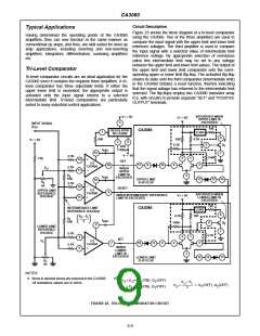
CA3060
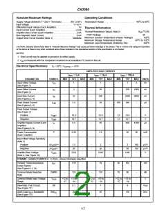
Absolute Maximum Ratings
Operating Conditions
o
o
Supply Voltage (Between V+ and V- Terminals). . . . . . . 36V (±18V)
Input Voltage. . . . . . . . . . . . . . . . . . . . . . . . . . . . . . . . . . . . . V+ to V-
Differential Input Voltage (Each Amplifier) . . . . . . . . . . . . . . . . . . 5V
Input Current (Each Amplifier) . . . . . . . . . . . . . . . . . . . . . . . . . . . . ±1mA
Amplifier Bias Current (Each Amplifier) . . . . . . . . . . . . . . . . . . .2mA
Bias Regulator Input Current . . . . . . . . . . . . . . . . . . . . . . . . . . -5mA
Output Short Circuit Duration (Note 1) . . . . . . . . . . . . . . . . Indefinite
Temperature Range . . . . . . . . . . . . . . . . . . . . . . . . . -40 C to 85 C
Thermal Information
o
Thermal Resistance (Typical, Note 2)
θJA ( C/W)
PDIP Package . . . . . . . . . . . . . . . . . . . . . . . . . . . . .
90
o
Maximum Junction Temperature (Plastic Package) . . . . . . . 150 C
Maximum Storage Temperature Range . . . . . . . . . -65 C to 150 C
Maximum Lead Temperature (Soldering 10s) . . . . . . . . . . . . 300 C
o
o
o
CAUTION: Stresses above those listed in “Absolute Maximum Ratings” may cause permanent damage to the device. This is a stress only rating and operation
of the device at these or any other conditions above those indicated in the operational sections of this specification is not implied.
NOTES:
1. Short circuit may be applied to ground or to either supply.
2. θ is measured with the component mounted on an evaluation PC board in free air.
JA
o
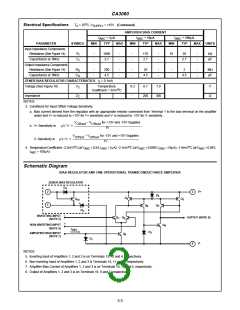
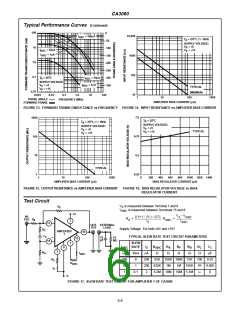
Electrical Specifications
T = 25 C, V
= ±15V
A
SUPPLY
AMPLIFIER BIAS CURRENT
= 10µA
I
= 1µA
I
I
= 100µA
ABC
ABC
ABC
PARAMETER
SYMBOL
MIN
TYP
MAX
MIN
TYP
MAX
MIN
TYP
MAX
UNITS
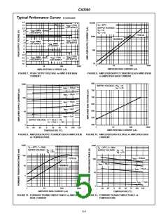
Input Offset Voltage
(See Figure 1)
V
-
-
-
-
1
3
-
-
1
-
-
1
5
mV
IO
Input Offset Current
(See Figure 2)
I
-
-
-
-
-
-
30
-
-
-
-
-
250
1000
5000
-
nA
nA
µA
IO
Input Bias Current
(See Figures 3, 4)
I
33
2.3
300
26
2500
240
IB
Peak Output Current
(See Figures 5, 6)
I
150
OM
Peak Output Voltage
(See Figure 7)
Positive
V
+
-
-
-
13.6
14.7
8.5
-
-
-
-
-
-
13.6
14.7
85
-
-
-
12
12
-
13.6
14.7
850
-
-
V
V
OM
Negative
V
-
OM
Amplifier Supply Current (Each
Amplifier)
I
1200
µA
A
(See Figures 8, 9)
Power Consumption
(Each Amplifier)
P
-
0.26
-
-
2.6
-
-
26
36
mW
Input Offset Voltage Sensitivity
(Note 3)
Positive
∆V /∆V+
IO
-
-
-
1.5
20
-
-
-
-
-
-
2
-
-
-
-
-
-
2
150
150
-
µV/V
µV/V
V
Negative
∆V /∆V-
IO
20
30
Amplifier Bias Voltage
(Note 4, See Figure 10)
V
0.54
0.60
0.66
ABC
DYNAMIC CHARACTERISTICS At 1kHz, Unless Otherwise Specified
Forward Transconductance
(Large Signal)
(See Figures 11, 12)
g
-
1.55
-
-
-
18
-
30
70
102
90
-
mS
21
Common Mode Rejection
Ratio
CMRR
-
110
-
-
-
-
110
-
-
-
-
-
-
-
-
dB
V
Common Mode Input Voltage
Range
V
+12 to +13 to
-12
+12 to +13 to
-12
+12 to +13 to
-12
ICR
-14
-14
-14
Slew Rate (Test Circuit)
(See Figure 17)
SR
-
0.1
-
1
-
8
V/µs
kHz
Open Loop (g ) Bandwidth
21
BW
OL
-
20
-
45
-
110
(See Figure 13)
3-2

 HARRIS [ HARRIS CORPORATION ]