CCD image sensors
S11510 series
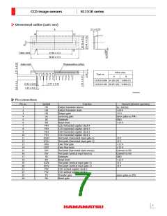
Dimensional outline (unit: mm)
3.3 0.35
A
24
13
12
1
Index mark
Index mark
27.94 0.3
38.10 0.4
Photosensitive surface
Active area
Type no.
A
B
S11510-1006 14.336 (H) 0.896 (V)
S11510-1106 28.672 (H) 0.896 (V)
2.54 0.13
0.46 0.05
1.27 0.2
KMPDA0265EA
Pin connections
Pin no.
1
Symbol
OS
OD
Function
Remark (standard operation)
RL=100 kΩ
+24 V
Output transistor source
Output transistor drain
Output gate
2
3
OG
+5 V
4
SG
Summing gate
Same pulse as P4H
5
SS
Substrate
GND
6
RD
Reset drain
+12 V
7
8
9
P4H
P3H
P2H
P1H
IG2H
IG1H
OFG
OFD
ISH
ISV
CCD horizontal register clock-4
CCD horizontal register clock-3
CCD horizontal register clock-2
CCD horizontal register clock-1
Test point (horizontal input gate-2)
Test point (horizontal input gate-1)
Over flow gate
10
11
12
13
14
15
16
17
18
19
20
21
22
23
24
-8 V
-8 V
+12 V
+12 V
Connect to RD
Connect to RD
GND
+12 V
-8 V
Over flow drain
Test point (horizontal input source)
Test point (vertical input source)
Substrate
SS
RD
Reset drain
IG2V
IG1V
P2V
P1V
TG
Test point (vertical input gate-2)
Test point (vertical input gate-1)
CCD vertical register clock-2
CCD vertical register clock-1
Transfer gate
-8 V
Same pulse as P2V
RG
Reset gate
7

 HAMAMATSU [ HAMAMATSU CORPORATION ]