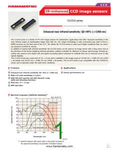
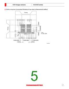
CCD image sensors
S11510 series
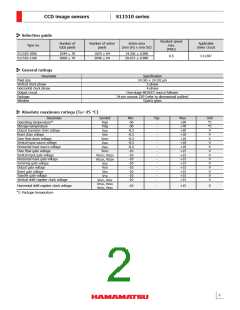
Selection guide
Readout speed
max.
Number of
total pixels
Number of active
pixels
Active area
Applicable
driver circuit
Type no.
[mm (H) mm (V)]
×
(MHz)
S11510-1006
S11510-1106
1044 70
1024 64
14.336 0.896
×
×
×
0.5
C11287
2068 70
2048 64
28.672 0.896
×
×
×
General ratings
Parameter
Specification
Pixel size
14 (H) 14 (V) μm
×
Vertical clock phase
Horizontal clock phase
Output circuit
Package
2-phase
4-phase
One-stage MOSFET source follower
24-pin ceramic DIP (refer to dimensional outline)
Quartz glass
Window
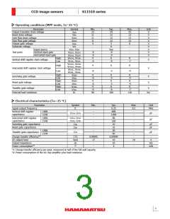
Absolute maximum ratings (Ta=25 °C)
Parameter
Operating temperature*2
Storage temperature
Output transistor drain voltage
Reset drain voltage
Over flow drain voltage
Vertical input source voltage
Horizontal input source voltage
Over flow gate voltage
Vertical input gate voltage
Horizontal input gate voltage
Summing gate voltage
Symbol
Topr
Tstg
VOD
VRD
VOFD
VISV
VISH
VOFG
Min.
-50
-50
-0.5
-0.5
-0.5
-0.5
-0.5
-10
-10
-10
-10
-10
-10
-10
-10
Typ.
Max.
+50
+70
+30
+18
+18
+18
+18
+15
+15
+15
+15
+15
+15
+15
+15
Unit
°C
°C
V
V
V
V
V
V
V
V
V
V
V
V
V
-
-
-
-
-
-
-
-
-
-
-
-
-
-
-
VIG1V, VIG2V
VIG1H, VIG2H
VSG
Output gate voltage
Reset gate voltage
Transfer gate voltage
Vertical shift register clock voltage
VOG
VRG
VTG
VP1V, VP2V
VP1H, VP2H
VP3H, VP4H
Horizontal shift register clock voltage
-10
-
+15
V
*2: Package temperature
2

 HAMAMATSU [ HAMAMATSU CORPORATION ]