PDF
最近搜索
热门搜索
发布采购

| 型号: | GS816273C-250 |
| PDF下载: | 下载PDF文件 查看货源 |
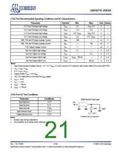
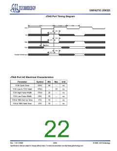
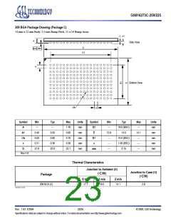
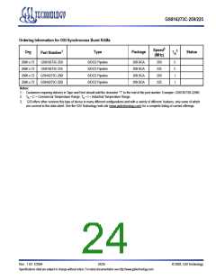
| 内容描述: | 256K X 72 18MB S / DCD同步突发静态存储器 [256K x 72 18Mb S/DCD Sync Burst SRAMs] |
| 分类和应用: | 存储静态存储器 |
| 文件页数/大小: | 25 页 / 516 K |
| 品牌: |  GSI [ GSI TECHNOLOGY ] GSI [ GSI TECHNOLOGY ] |
专业IC领域供求交易平台:提供全面的IC Datasheet资料和资讯,Datasheet 1000万数据,IC品牌1000多家。