GS816273C-250/225
JTAG Port Recommended Operating Conditions and DC Characteristics
Parameter
Symbol
Min.
2.0
Max.
Unit Notes
V
V
V
+0.3
DD3
3.3 V Test Port Input High Voltage
3.3 V Test Port Input Low Voltage
2.5 V Test Port Input High Voltage
2.5 V Test Port Input Low Voltage
TMS, TCK and TDI Input Leakage Current
TMS, TCK and TDI Input Leakage Current
TDO Output Leakage Current
V
V
1
1
IHJ3
V
–0.3
0.8
+0.3
ILJ3
V
0.6 * V
V
1
IHJ2
DD2
DD2
V
0.3 * V
1
–0.3
–300
–1
V
1
ILJ2
DD2
I
uA
uA
uA
V
2
INHJ
I
100
1
3
INLJ
I
–1
4
OLJ
V
Test Port Output High Voltage
1.7
—
5, 6
5, 7
5, 8
5, 9
OHJ
V
Test Port Output Low Voltage
—
0.4
V
OLJ
V
V
– 100 mV
DDQ
Test Port Output CMOS High
—
V
OHJC
V
Test Port Output CMOS Low
—
100 mV
V
OLJC
Notes:
1. Input Under/overshoot voltage must be –2 V > Vi < V
+2 V not to exceed 4.6 V maximum, with a pulse width not to exceed 20% tTKC.
DDn
2.
V
≤ V ≤ V
ILJ
IN
DDn
3. 0 V ≤ V ≤ V
IN
ILJn
4. Output Disable, V
= 0 to V
DDn
OUT
5. The TDO output driver is served by the V
supply.
DDQ
6.
7.
8.
9.
I
I
I
I
= –4 mA
OHJ
= + 4 mA
OLJ
= –100 uA
= +100 uA
OHJC
OHJC
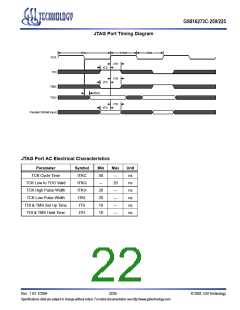
JTAG Port AC Test Conditions
Parameter
Input high level
Conditions
2.3 V
JTAG Port AC Test Load
DQ
Input low level
0.2 V
*
Input slew rate
1 V/ns
50Ω
30pF
Input reference level
Output reference level
1.25 V
V = 1.25 V
T
1.25 V
* Distributed Test Jig Capacitance
Notes:
1. Include scope and jig capacitance.
2. Test conditions as as shown unless otherwise noted.
Rev: 1.03 7/2004
21/25
© 2002, GSI Technology
Specifications cited are subject to change without notice. For latest documentation see http://www.gsitechnology.com.

 GSI [ GSI TECHNOLOGY ]