GS816273C-250/225
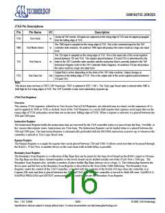
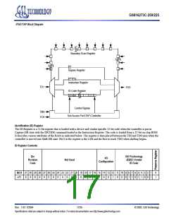
JTAG TAP Block Diagram
·
·
·
·
·
·
·
·
Boundary Scan Register
·
·
·
0
Bypass Register
2
1 0
Instruction Register
TDI
TDO
ID Code Register
31 30 29
2 1
0
·
· · ·
Control Signals
Test Access Port (TAP) Controller
TMS
TCK
Identification (ID) Register
The ID Register is a 32-bit register that is loaded with a device and vendor specific 32-bit code when the controller is put in
Capture-DR state with the IDCODE command loaded in the Instruction Register. The code is loaded from a 32-bit on-chip ROM.
It describes various attributes of the RAM as indicated below. The register is then placed between the TDI and TDO pins when the
controller is moved into Shift-DR state. Bit 0 in the register is the LSB and the first to reach TDO when shifting begins.
ID Register Contents
Die
Revision
Code
GSI Technology
JEDEC Vendor
ID Code
I/O
Not Used
Configuration
Bit # 31 30 29 28 27 26 25 24 23 22 21 20 19 18 17 16 15 14 13 12 11 10 9 8 7 6 5 4 3 2 1
x72 0 1 1 0 1 1 0 0 1
0
1
X
X
X
X
0
0
0
0
0
0
0
0
0
0
0
0
1
0
0
1
0
0
Rev: 1.03 7/2004
17/25
© 2002, GSI Technology
Specifications cited are subject to change without notice. For latest documentation see http://www.gsitechnology.com.

 GSI [ GSI TECHNOLOGY ]