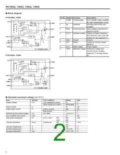
FA13842, 13843, 13844, 13845
■ Recommended operating conditions
Item
Symbol
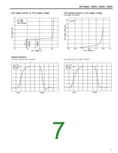
VCC
Min.
10
Max.
25
Unit
V
Supply voltage
Oscillation timing capacitor
Oscillation timing resistor
Oscillation frequency
CT
0.47
2.0
10
10
nF
RT
100
500
kΩ
kHz
fOSC
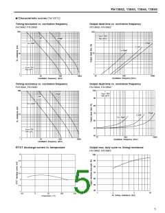
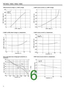
■ Electrical characteristics (Vcc=15V, RT=10kΩ, CT=3.3nF, Ta=25˚C)
Reference voltage section
Item
Symbol
VREF
LINE
Test condition
Tj=25˚C, IL=1mA
Vcc=10 to 25V
IL=0 to 20mA
Ta=–25 to 85˚C
Tj=25˚C
Min.
Typ.
5.00
±3
Max.
5.25
±20
Unit
V
Reference voltage
Line regulation
4.75
mV
Load current regulation
Temperature regulation
Output current at short-circuit
LOAD
VTC
±3
±25
mV
±0.3
60
mV/˚C
mA
IOS
Oscillator section
Item
Symbol
Test condition
Tj=25˚C
Min.
49
Typ.
Max.
55
Unit
kHz
kHz
%
Oscillation frequency
fOSC
52
Ta=–25 to 85˚C
Vcc=10 to 25V
Ta=–25 to 85˚C
Tj=25˚C
47
57
Voltage stability
fdv
±0.25
–0.07
1.6
±1
Temperature stability
Oscillation amplitude
Discharge current
fdt
%/˚C
V
VOSC
IDISCHG
Tj=25˚C
8.4
mA
Error amplifier section
Item
Symbol
VFB
Test condition
Min.
Typ.
Max.
2.6
Unit
V
Input voltage
COMP=2.5V, Tj=25˚C
2.4
2.5
Input leak current
Open-loop gain
Unity gain bandwidth
Output source current
Output sink current
Output voltage
IFB
±2
µA
AV
65
72
1
dB
fT
0.7
–0.8
2
MHz
mA
mA
V
ISOURCE
ISINK
FB=2.3V, COMP=0V
–1.0
15
4.5
80
FB=2.7V, COMP=1V
VH COMP
VL COMP
FB=2.3V, RL=15kΩ to GND
FB=2.7V, RL=15kΩ to VREF
4.0
500
mV
Current sensing section
Item
Symbol
AV IS
VTH IS
IIS
Test condition
Tj=25˚C
Min.
2.85
0.9
Typ.
3
Max.
3.15
1.1
Unit
V/V
V
Voltage gain
Maximum input signal
Input bias current
Delay to output
FB=0V
1.0
–1
–5
µA
ns
TPD
Tj=25˚C, ISNS to OUT
150
300
3

 FUJI [ FUJI ELECTRIC ]