FA13842, 13843, 13844, 13845
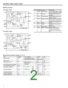
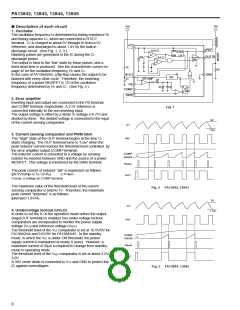
■ Block diagram
Á FA13842, 13843
Pin No. Symbol Function
Description
1
2
3
4
COMP Compensating
Error amplifier output, available
for loop compensation circuit
Inverting input of the error
amplifier
7
VCC
UVLO
VCC
ENB
8
6
VREF
OUT
5V REF
2.5V
30V
FB
Feedback
UVLO
OUTPUT
ENB
ISNS
Current sensing
Input voltage proportional to
inductor current
RT/CT Oscillator control Setting oscillation frequency
and maximum duty-cycle with
RT/CT
4
OSC
5
GND
resistor RT and capacitor CT
ER AMP
5
6
GND
OUT
Ground
Output
Ground
2
1
FB
2R
1R
Output for driving a power
MOSFET
COMP
1V
S
Q
FF
QB
R
ISNS
7
8
VCC
Power supply
Power supply
3
VREF
Reference voltage Reference voltage and
current source charging
capacitor CT through resistor
RT
5V Controlled block
Á FA13844, 13845
7
VCC
UVLO
VREF
OUT
VCC
ENB
8
6
5V REF
2.5V
30V
UVLO
OUTPUT
ENB
4
RT/CT
OSC
5
GND
ER AMP
2
1
FB
2R
1R
COMP
1V
TFF
Q
S
R
Q
FF
CLK
QB
QB
ISNS
3
5V ControlIed block
■ Absolute maximum ratings (Ta=25˚C)
Item
Symbol
Test condition
Rating
Unit
Supply voltage
VCC
Low impedance source
Zener clamp (Icc<10mA)
28
V
Self limiting
10
V
Zener current
IZ
mA
mA
A
Output peak current
IO
Source current
Sink current
FB, ISNS
400
1
FB/ISNS terminal input voltage
Error amplifier sink current
Total power dissipation
VIN
ISINK
Pd
–0.3 to 5.3
10
V
mA
mW
at Ta < 50˚C
Junction-air
DIP
800
SOP
DIP
400
Thermal resistance
R
θ
j-a
125
˚C/W
SOP
250
Junction temperature
Ambient temperature
Storage temperature
Tj
150
˚C
˚C
˚C
Ta
–25 to 85
–40 to 150
Tstg
2

 FUJI [ FUJI ELECTRIC ]