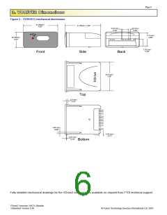
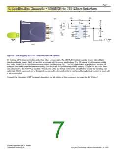
Page ꢃ
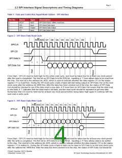
checꢅed to see iꢇ the data read was accepted. ꢄ ꢃ0ꢀ level on ꢂꢌI Data ꢆut means that the data write was accepted. ꢄ
ꢃ1ꢀ indicates that the internal ꢁuꢇꢇer is ꢇullꢈ and the write should ꢁe repeated. ꢋememꢁer that Cꢂ must ꢁe held low ꢇor at
least one clocꢅ period ꢁeꢇore ꢁeing taꢅen high again to continue with the neꢉt read or write cycle.
Figure 4 - ꢂꢌI ꢂlave Data Timing Diagrams
T1
SPICLK
T2
T3
SPICS /
SPI DATA IN
T6
T4
T5
SPI DATA OUT
T7
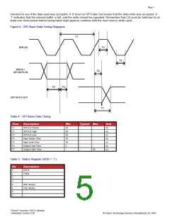
Taꢁle 4 - ꢂꢌI ꢂlave Data Timing
Time
T1
Description
ꢂꢌICLK ꢌeriod
ꢂꢌICLK High
Min
83
20
20
10
10
2
Typical Max
Unit
ns
-
-
-
-
-
-
-
-
T2
-
ns
T3
ꢂꢌICLK Low
-
ns
T4
Input ꢂetup Time
Input Hold Time
ꢆutput Hold Time
ꢆutput Valid Time
-
ns
Tꢍ
-
ns
T6
-
ns
T7
-
20
ns
Taꢁle ꢍ - ꢂtatus ꢋegister (ꢄDD = ꢃ1ꢀ)
Bit
0
Description
RXF#
1
TXE#
2
-
3
-
4
RXF IRQEn
ꢍ
TXE IRQEn
6
-
-
7
VDrive2 Vinculum VNC1L Module
Datasheet Version 0.99
© Future Technology Devices International Ltd. 2007

 FTDI [ FUTURE TECHNOLOGY DEVICES INTERNATIONAL LTD. ]