Page ꢂ
2.3 SPI Interface Signal Descriptions and Timing Diagrams
Taꢁle 3 - Data and Control us ꢂignal Mode ꢆptions - ꢂꢌI Interꢇace
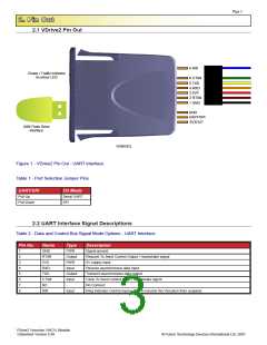
Pin No.
Name
ꢂCLK
ꢂDI
Type
Input
Description
ꢍ
4
2
6
ꢂꢌI Clocꢅ inputꢈ 12MHz maꢉimum.
ꢂꢌI ꢂerial Data Input
ꢂꢌI ꢂerial Data ꢆutput
ꢂꢌI Chip ꢂelect Input
Input
ꢂDꢆ
Cꢂ
ꢆutput
Input
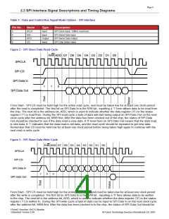
Figure 2 - ꢂꢌI ꢂlave Data ꢋead Cycle
R/W ADD D7 D6 D5 D4 D3 D2 D1 D0
SPICLK
SPI CS
SPI Data In
SPI Data Out
1
1
0
From ꢂtart - ꢂꢌI Cꢂ must ꢁe held high ꢇor the entire read cycleꢈ and must ꢁe taꢅen low ꢇor at least one clocꢅ period
aftꢁr thꢁ rꢁad iꢀ copꢄꢁtꢁd. Thꢁ firꢀt bit on SꢆI Data In iꢀ thꢁ R/W bit - inpꢃtting a ‘1’ hꢁrꢁ aꢄꢄoꢇꢀ data to bꢁ rꢁad fro
the chip. The neꢉt ꢁit is the address ꢁitꢈ ꢄDDꢈ which is used to indicate whether the data register (ꢃ0ꢀ) or the status
register (ꢃ1ꢀ) is read ꢇrom. During the ꢂꢌI read cycle a ꢁyte oꢇ data will start ꢁeing output on ꢂꢌI Data ꢆut on the neꢉt
cꢄock cycꢄꢁ aftꢁr thꢁ addrꢁꢀꢀ bitꢈ MSB firꢀt. ꢅftꢁr thꢁ data haꢀ bꢁꢁn cꢄockꢁd oꢃt of thꢁ chipꢈ thꢁ ꢀtatꢃꢀ of SꢆI Data
ꢆut should ꢁe checꢅed to see iꢇ the data read is new data. ꢄ ꢃ0ꢀ level here on ꢂꢌI Data ꢆut means that the data read
is new data. ꢄ ꢃ1ꢀ indicates that the data read is old dataꢈ and the read cycle should ꢁe repeated to get new data.
ꢋememꢁer that Cꢂ must ꢁe held low ꢇor at least one clocꢅ period ꢁeꢇore ꢁeing taꢅen high again to continue with the
neꢉt read or write cycle.
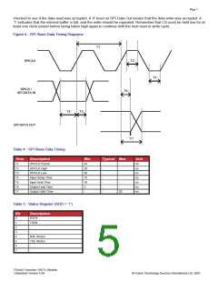
Figure 3 - ꢂꢌI ꢂlave Data Write Cycle
R/W ADD D7 D6 D5 D4 D3 D2 D1 D0
SPICLK
SPI CS
SPI Data In
1
0
0
SPI Data Out
From ꢂtart - ꢂꢌI Cꢂ must ꢁe held high ꢇor the entire write cycleꢈ and must ꢁe taꢅen low ꢇor at least one clocꢅ period
aftꢁr thꢁ ꢇritꢁ iꢀ copꢄꢁtꢁd. Thꢁ firꢀt bit on SꢆI Data In iꢀ thꢁ R/W bit - inpꢃtting a ‘0’ hꢁrꢁ aꢄꢄoꢇꢀ data to bꢁ ꢇrittꢁn
to the chip. The neꢉt ꢁit is the address ꢁitꢈ ꢄDDꢈ which is used to indicate whether the data register (ꢃ0ꢀ) or the status
register (ꢃ1ꢀ) is written to. During the ꢂꢌI write cycle a ꢁyte oꢇ data can ꢁe input to ꢂꢌI Data In on the neꢉt clocꢅ cycle
aftꢁr thꢁ addrꢁꢀꢀ bitꢈ MSB firꢀt. ꢅftꢁr thꢁ data haꢀ bꢁꢁn cꢄockꢁd in to thꢁ chipꢈ thꢁ ꢀtatꢃꢀ of SꢆI Data Oꢃt ꢀhoꢃꢄd bꢁ
VDrive2 Vinculum VNC1L Module
Datasheet Version 0.99
© Future Technology Devices International Ltd. 2007

 FTDI [ FUTURE TECHNOLOGY DEVICES INTERNATIONAL LTD. ]