FT260 HID-CLASS USB TO UART/I2C BRIDGE IC
Version 1.1
Document No.: FT_001272 Clearance No.: FTDI#484
The FT260 provides a bridge which connects a “HID-over-I²C” device via an I²C bus, helps to translate
USB HID requests from a PC to the device, and makes it work as a normal USB HID class device. With
the FT260, an I2C slave function compliant to HID-over-I2C protocol can directly communicate to USB
HID class driver through the USB connection.
Configurable Settings for Customization. An electrical poly-fuse (eFUSE) is embedded in the FT260.
This embedded eFUSE provides the configurable settings of the Vendor Specific Parameters for basic
customization. These Vendor Specific Parameters are the settings about USB, I/O and HID-over-I2C.
Users can utilize this embedded eFUSE to achieve basic customization.
For advanced settings, the FT260 also reserves the programming interface of an external EEPROM via an
I2C interface to record the Vendor Specific Parameters. The FT260 will automatically scan for the
presence of an EEPROM. (See Supported EEPROM Spec for suitable devices). When the FT260 is powered
up, these Vendor Specific Parameters will be automatically loaded and the FT260 will operate with the
parameter setting. When both eFUSE and EEPROM exist at the same time, the Vendor Specific
Parameters in the EEPROM will dominate. Both eFUSE and EEPROM can be programmed using the FTDI
utility software called FT_PROG, which can be downloaded from the FTDI Utilities page on the FTDI
website
(http://www.ftdichip.com/Support/Utilities.htm#FT_Prog).
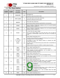
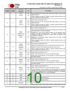
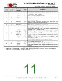
Configurable Digital I/Os. There are 14 digital pins in the FT260 that can be configured for different
purposes, such as UART/I2C bus signals, General Purpose Input/Output (GPIO), LED indicator for data
transfer over UART, a USB suspend indicator output, remote wake up input, an interrupt input or power
enable indicator. Functions for each pin will be determined during Chip Configuration, with parameters
from the eFUSE or EEPROM, or via USB commands.
The signal drive strength of these Digital I/Os can be configured via the FT_Prog utility for different
design needs.
Power management. The operating clock for the FT260 can be set as 48MHz, 24MHz, 12MHz. Higher
operating frequencies allow higher data throughput. And, lower operating frequencies allow lower power
consumption. IDLE mode is also supported and can be enabled via the parameters in eFUSE or EEPROM.
The system operating clock will be switched to 30 kHz when no data is transferred between USB and
I2C/UART bus for a period of 5 seconds. Any UART RX signalling will trigger the whole chip exiting from
the IDLE mode to normal operating status.
USB suspend/resume and remote wakeup are fully supported. The FT260 will be set to a power saving
status and the clock to most of the digital circuits will be stopped when the device is suspended.
Source Power and Power Consumption. The FT260 is capable of operating with a voltage supply of
+3.3V or +5.0V with a nominal operational mode current of 24mA, a nominal idle mode current of 5.6mA
and a nominal USB suspend mode current of 405µA. This allows greater margin for peripheral designs to
meet the USB suspend mode current limit of 2.5mA. An integrated level converter within the FT260
allows the device to interface with logic running at +1.8V, 2.5V or +3.3V. (Note: External pull-ups are
recommended for IO <3V3).
4.2 Functional Block Descriptions
The following paragraphs detail each function within the FT260. Please refer to the block diagram shown
in Figure 2.1 .
Internal Oscillator. The Internal Oscillator cell generates a 48MHz reference clock. With internal
trimming mechanisms and an adaptive algorithm, this oscillator provides a stable clock source to the USB
DPLL block for generating a recovered clock to Clock Synthesizer block for functional operating.
Clock Synthesizer. The Clock Synthesizer takes the 48MHz clock from the Internal Oscillator and
Copyright © Future Technology Devices International Limited
13

 FTDI [ FUTURE TECHNOLOGY DEVICES INTERNATIONAL LTD. ]