FT260 HID-CLASS USB TO UART/I2C BRIDGE IC
Version 1.1
Document No.: FT_001272 Clearance No.: FTDI#484
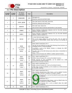
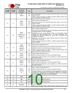
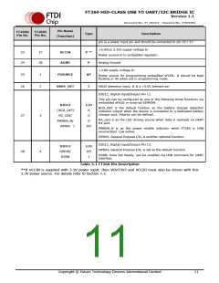
Pin Name
FT260Q
Pin No.
FT260S
Pin No.
Type
Description
(Function)
pin is a power input pin and should be connected to pin 23 / 27.
+5.0V(or 3.3V) supply voltage In
23
24
27
28
VCCIN
AGND
P **
Power source-in to embedded regulator.
P
Analog Ground
+3.8V supply voltage In
25
26
1
2
FSOURCE
AP
I
Power source for programming embedded eFUSE. It should be kept
floating or 0V when not in programming mode
VBUS_DET
VBUS detection input. It is a +5.0V tolerant pin
DIO12, Digital Input/Output Pin 12.
This pin can be configured as one of the following three functions via
embedded eFUSE or external EEPROM.
DIO12
( BCD_DET/
RX_LED/
I/O
O
BCD_DET is the default function as the battery charger detection
indicator output when the device is connected to a dedicated battery
charger port. Polarity can be defined.
27
3
O
RX_LED is as the LED driving source when data is received on UART
RX port.
PWREN_N/
O
GPIOG
)
I/O
PWREN_N is as the power enable indicator when FT260 is USB
enumerated. Low active.
GPIOG, General Purpose I/O, is another optional function.
DIO13, Digital Input/Output Pin 13.
DIO13
GPIOH/
DSRN
I/O
I/O
I
GPIOH, General Purpose I/O, is set as the default function
28
4
DSRN, Data Set Ready, can be enabled via USB command for UART
interface.
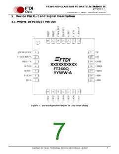
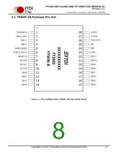
Table 3.1 FT260 Pin Description
**If VCCIN is supplied with 3.3V power input, then VOUT3V3 and VCCIO must also be driven with this
3.3V power source. For details refer to Section 7.3.
Copyright © Future Technology Devices International Limited
11

 FTDI [ FUTURE TECHNOLOGY DEVICES INTERNATIONAL LTD. ]